28.07.2021 polprog. Moved 06.02.2022
jumptable: The hardware — Blink — 8051 software core — First peripheral — Running on real hardware — UART Tx — bin2memh — First assembled program
I bought it earlier this year, and after playing with Verilog on the Spartan 6 boards, I decided to play with this one
First of all I had to compile the toolchain, which is yosys for synthesis, nextpnr-ecp5 for place and route, and Trellis for bitstream generation
Then I adapted the blink example from prjtrellis examples with my verilog, their makefile and their lpf file (i had to understand the non-verilog part because it was different that Xilinx ISE toolchain I was using on Spartan 6)
The blink1 project is a simple example to get started.
I wanted to try some software core on the FPGA. I chose 8051 because it's a simple CPU and the machine code can be written by hand. I found two Verilog implementations:
I decided to go with the first one as it had something of a readme (neither is documented very well, but risclite's example has a working simulation). The simulation was a very valuable resource as it showed me exactly how to interact with the 8051 block. It is worth to mention that this is not the 8051 microcontroller, but only the 8051 CPU core. Fortunately the simulation implemented enough to run a small binary from ROM.This approach is extremely flexible, because I can implement any peripheral I want, while keeping the simplicity of the 8051 core available. I can write my custom peripherals in verilog and compile C programs for 8051 to interface with them. This allows me to describe my very own microcontroller, with virtually any peripheral I want.
I started by running the existing simulation in Icarus Verilog and using gtkwave to view the traces. I had to modify the simulation module, but through experimenting I started to understand how to use the softcore block.
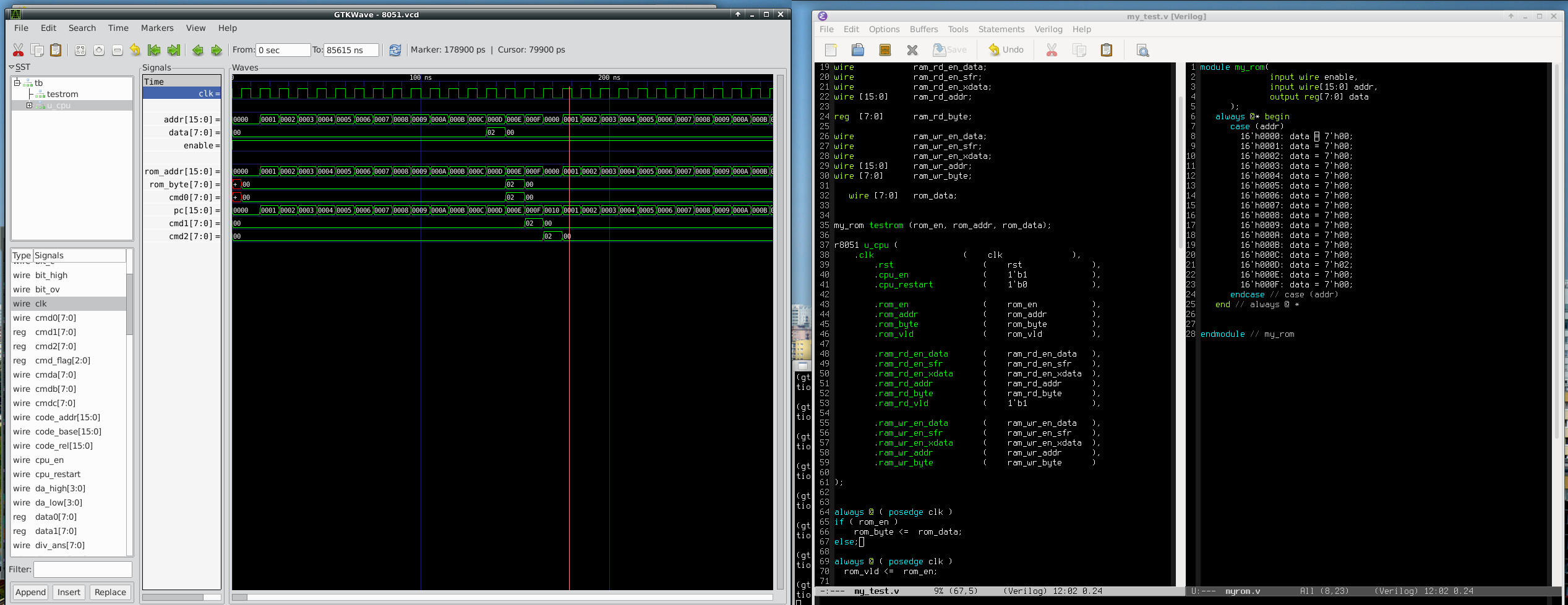
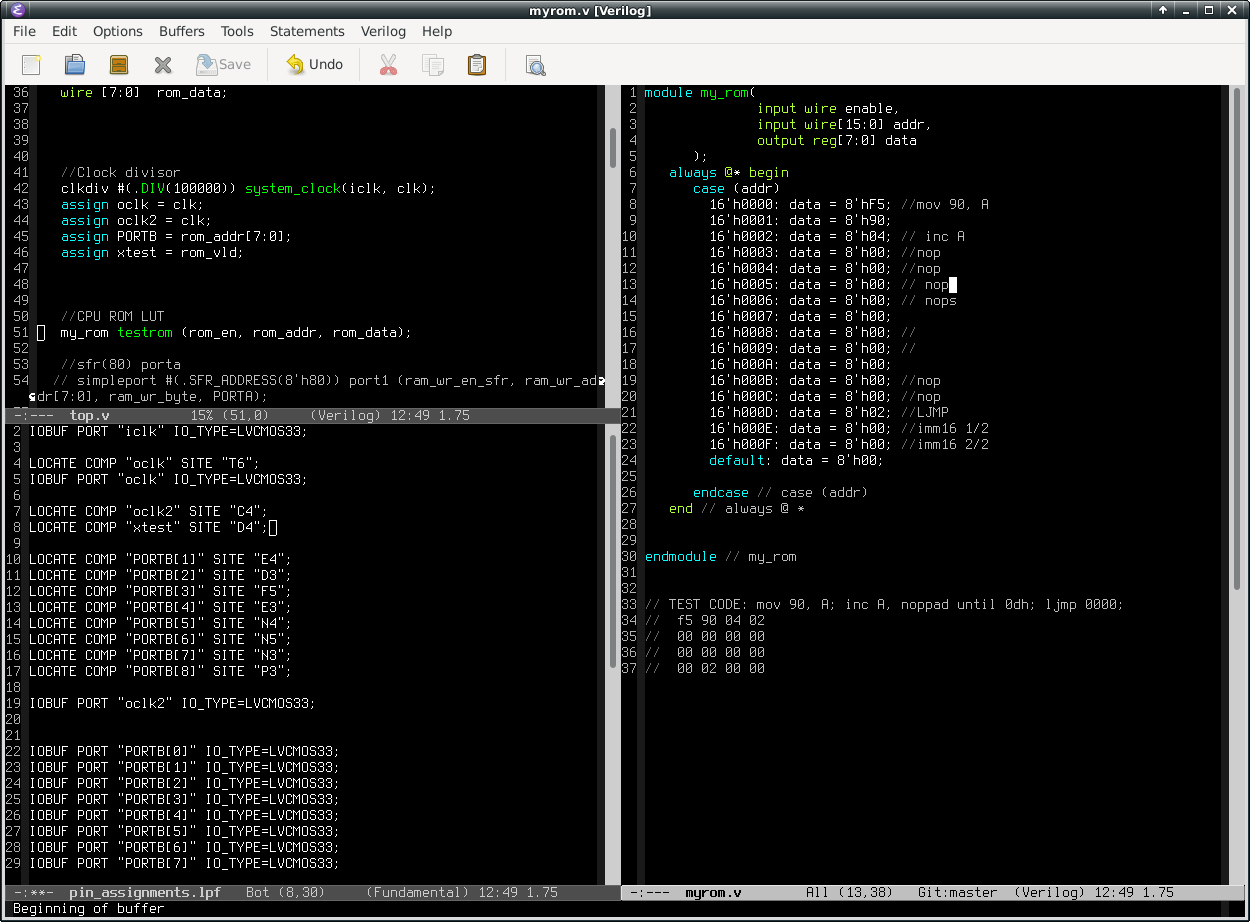
I implemented my ROM as a verilog Lookup table (simply a 16 case switch statement). The module is listed below:
my8051/myrom.v
module my_rom(
	      input wire enable,
	      input wire[15:0] addr,
	      output reg[7:0] data
      );
   always @* begin
      case (addr)
	16'h0000: data = 8'hF5; //mov 90, A
	16'h0001: data = 8'h90;
	16'h0002: data = 8'h04; // inc A
	16'h0003: data = 8'h00; //nop
	16'h0004: data = 8'h00; //nop
	16'h0005: data = 8'h00; // nop
	16'h0006: data = 8'h00; // nops
	16'h0007: data = 8'h00;
	16'h0008: data = 8'h00; //
 	16'h0009: data = 8'h00; //
	16'h000A: data = 8'h00;
	16'h000B: data = 8'h00; //nop
	16'h000C: data = 8'h00; //nop
	16'h000D: data = 8'h02; //LJMP
	16'h000E: data = 8'h00; //imm16 1/2
	16'h000F: data = 8'h00; //imm16 2/2
	default: data = 8'h00;

      endcase // case (addr)
   end // always @ *


endmodule // my_rom


// TEST CODE: mov 90, A; inc A, noppad until 0dh; ljmp 0000;
//  f5 90 04 02
//  00 00 00 00
//  00 00 00 00
//  00 02 00 00
The code in the ROM simply writes subsequent values to sfr 90 (later I put a peripheral there) Then I just had to connect it to the CPU core:
module top8051 ( /*...*/ );
   reg         clk;
   reg 	       rst = 1'b0;

   wire        rom_en;
   wire [15:0] rom_addr;
   reg [7:0]   rom_byte;
   reg 	       rom_vld;

   // ...

   wire [7:0]  rom_data;

   // ...

   //CPU ROM LUT
   my_rom testrom (rom_en, rom_addr, rom_data);

   // ...
   //Loading bytes from rom
   always @ ( posedge clk )
     if ( rom_en )
       rom_byte <=  rom_data;
     else;
   //ROM data valid signal
   always @ ( posedge clk )
     rom_vld <=  rom_en;
With that code, the CPU would load the ROM bytes from the LUT (in this case, it's a series
of NOPs and a LJMP) and execute the program stored it it:
Here, the minimal CPU+ROM machine is running a different ROM, changing some value in it's accumulator register ("acc" in the trace):
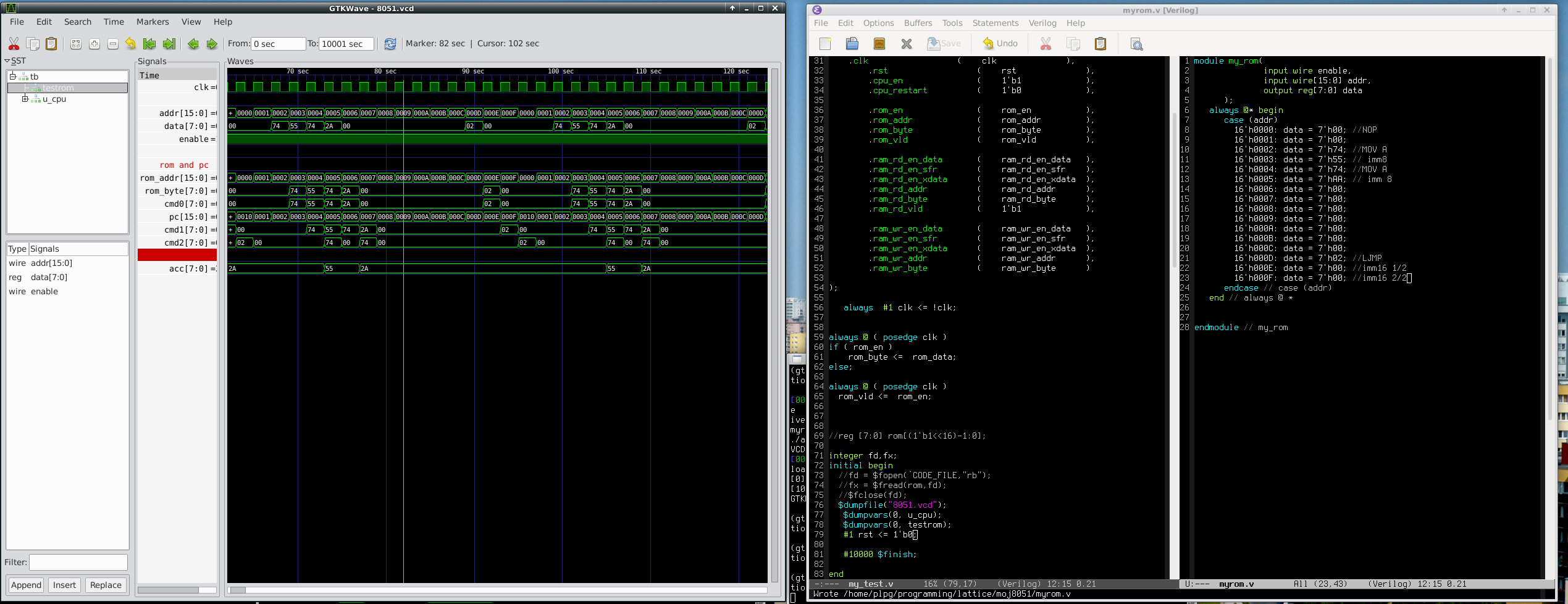
There is a bug in that screenshot (that I fixed later) as the data constants are 7 bits long, and they should be 8. This is why the wrong immediate value is loaded into the accumulator (2A instead of AA).
After reading the code and understanding it further, I was able to implement the simplest peripheral - a parallel output. Before we do this though, we have to understand how the core interfaces with the outer world. It happens through the address and data bus signals, just like on a real bare CPU IC.
The core uses a simple Verilog interface for the RAM:
      wire        ram_rd_en_data;   //Ram READ Data enable (internal RAM)
      wire        ram_rd_en_sfr;    //Ram READ SFR enable
      wire        ram_rd_en_xdata;  //Ram READ XRAM enable
      wire [15:0] ram_rd_addr;      //The address

      reg [7:0]   ram_rd_byte;      //The data

      wire        ram_wr_en_data;   //
      wire        ram_wr_en_sfr;    //
      wire        ram_wr_en_xdata;  //
      wire [15:0] ram_wr_addr;      //
      wire [7:0]  ram_wr_byte;      // Same as above but for writes.
For a read operation the CPU puts out the address in ram_rd_addr, and enables one of
the ram_rd_en_* lines. Which line is enabled depends on the address:
For example when the ROM byte becomes the E5 04 sequence (instruction mov A, 04), which is an IRAM read, the signal ram_rd_en_data momentarily goes high to indicate that an IRAM read is being performed. Similarly, when the ROM byte sequence is F5 80 (mov 80, A), which is an SFR write (remember the address range), the ram_wr_en_sfr goes high. Note that the bus control is driven when the CPU reads the second operand - the address.
A write operation is similar, address and data go into the ram_wr_addr and ram_wr_byte, and the corresponding ram_wr_en_* is set high.
With this, I know how to implement my own output peripheral. I need a block that:
module simpleport #(parameter SFR_ADDRESS = 8'h80) (
	   input 	    ram_wr_en_sfr,
	   input [7:0] 	    ram_wr_addr,
	   input [7:0] 	    ram_wr_byte,
	   output reg [7:0] out
	   );

   initial begin
      out <= 8'b0;
   end

   always @ (posedge ram_wr_en_sfr ) begin
      if(ram_wr_addr == SFR_ADDRESS) begin
	 out <= ram_wr_byte;
	 $display("Testport2@%2h: write %2h", SFR_ADDRESS, out);
      end


   end
endmodule
This block does exactly what is described in the list above. Now I have to connect it to the CPU...
simpleport #(.SFR_ADDRESS(8'h90)) port1 (ram_wr_en_sfr, ram_wr_addr[7:0], ram_wr_byte, PORTB);
... and add an output to my top8051 block:
module top8051(
	  input wire 	    iclk,
          output wire [7:0] PORTB,
);
With that, any SFR write to port 90h will appear on PORTB.
We need some test code:
0000h:
      mov 90, A
      inc A
      inc A
      inc A
      inc A
      inc A
      inc A
      inc A
      ljmp 0000h

ROM contents: F5 90 04 04 04 04 04 04 04 02 00 00
It's a simple routine, it copies the value of A to sfr(90h), which is our output port, and then increments A seven times. This will produce subsequent numbers on the output every 7 values.
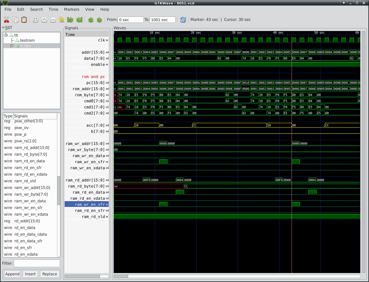
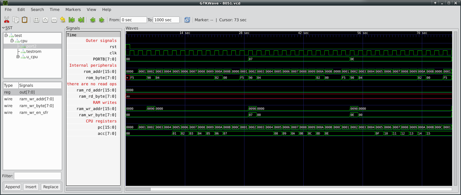
Here is the peripheral working in the simulator:
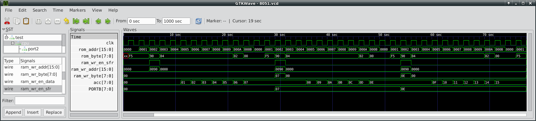
From the top there is the CPU clock, then goes the ROM address that is being read and the ROM data (the instruction). Below that, ram_wr_en_sfr indicates a write to an SFR at the address specified by ram_wr_addr of the value ram_wr_byte. You can see that on the rising edge of ram_wr_en_sfr the value of Accumulator (acc) is copied to ram_wr_byte and appears on PORTB output.
The peripheral works and it's outputting the values written to it's SFR!
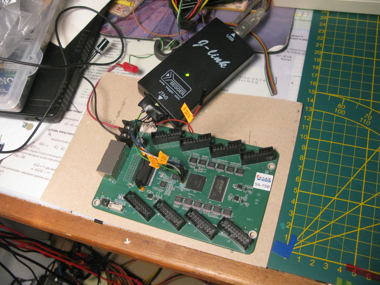
So far all of this was running in Icarus Verilog simulator. It's a very useful tool as you can inspect every signal, and recompilation does not take much time. However in order to make it work on real hardware some changes must be done. The clock needs to be connected to the real onboard clock signal, instead of an internally generated one, and the IO needs to be mapped to FPGA pins.
Fortunately on this board, all it took was to make a clock divider module (to be able to adjust the 8051 speed) and hardwire the rom_vld signal to 1 (I will change the ROM LUT later to drive that signal accordingly)
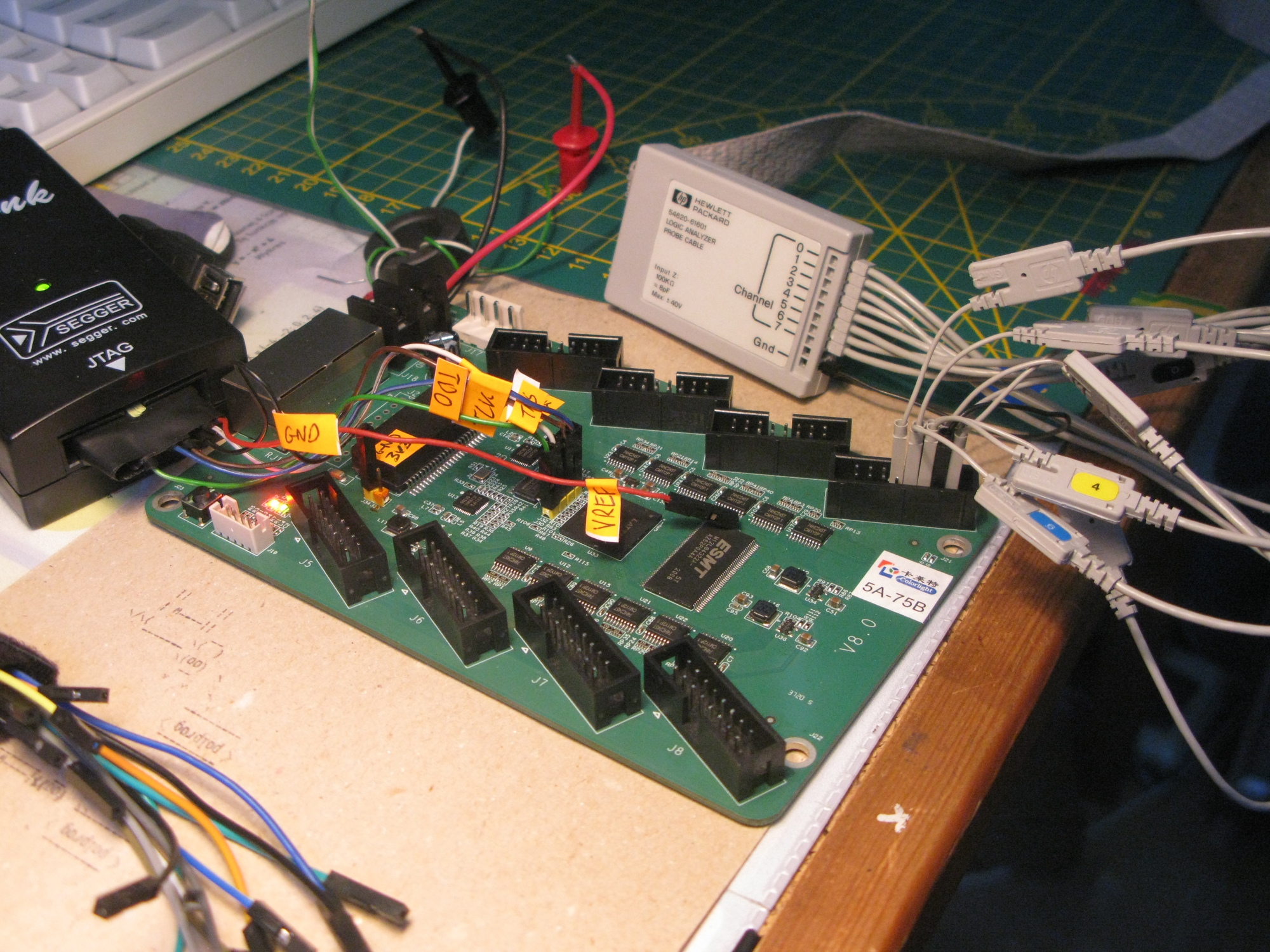
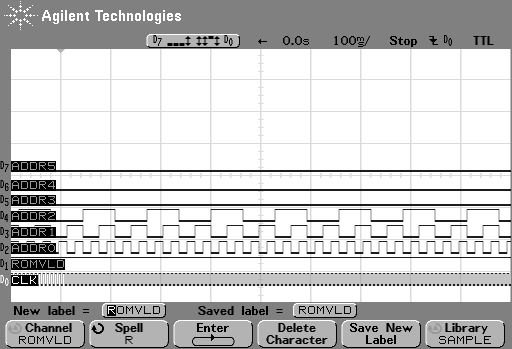
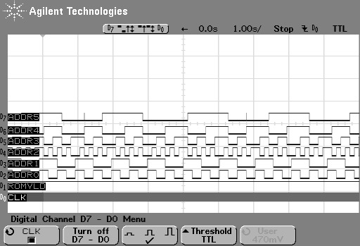
For testing I connected the ROM address to "PORTB" to figure out if the CPU was executing code at all. Here is the logic analyzer trace, the core is executing the LUT ROM from the picture above:
When I got that working, I connected the actual peripheral to the outputs, and put the test code back into the ROM
This is how PORTB changes running on real hardware (excuse me forgetting to update the signal labels, ADDRn should be PORTBn :) ). Notice how the time scale changed.
Below is the simulation again with some more signals displayed. You can see how helpful simulations are, as the logic analyzer on real hardware can only show CLK and PORTB (unless you specifically route other signals to the top - which certainly is possible to do)
At first I had a UART peripheral that was relatively simple and worked fine in the simulation. Unfortunately it had several clock domains and did not work at all on the FPGA.
The peripheral had to be completely rewritten to work on the real FPGA. The original code contained two different clocks in three always@ blocks. A baud clock that was clocking the transmitter FSM was generated based on the main system clock iclk. The new code does everything in a single always@ block clocked from iclk and now works flawlessly. The baudrate divisor is set to a fixed value but this will be implemented as a separate SFR.
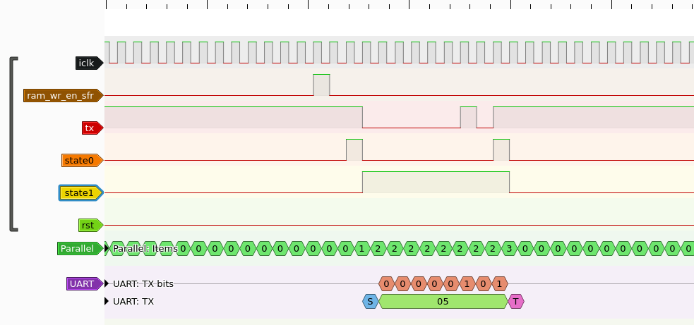
In the image above all important signals from the UART perupheral were carried out to the FPGA's physical output pins. tx is the output of the UART, state0 and state1 are the FSM state bits (also decoded with the Paralell decoder on the bottom. The tx line is decoded with pulseview's UART decoder, showing a transmitted 0x05 bit
In order to continue I needed an easier way to write test programs for the 8051. I decided to use sdcc toolchain to assemble assembly files (and later compile C) into something that can be put into a ROM lookup table in the 8051 core and eventually be executed. This turned out to be more complicated than I thought, mostly because of file format incompatoabilities. Verilog has a command to read from file into a LUT, but the format is unlike anything other used by standard toolchains. $readmemb and $readmemh are used to load flat files into LUTs. The latter one supposedly reads a "hex file", however it's not compatible with an Intel Hex format. Instead, it expects ASCII hex values separated by values, For example the assembly code
  nop
  nop
  nop
  mov 0x91, A
  inc a
would become
  00 00 00 f5 91
  04
The format supports //comments too. The script I wrote is here and the Makefile that turns the .s into a .mem is here.
While debugging this setup I made the 8051 output the ROM bytes on one of the HUB75 headers. Here is the final result when I got it all working
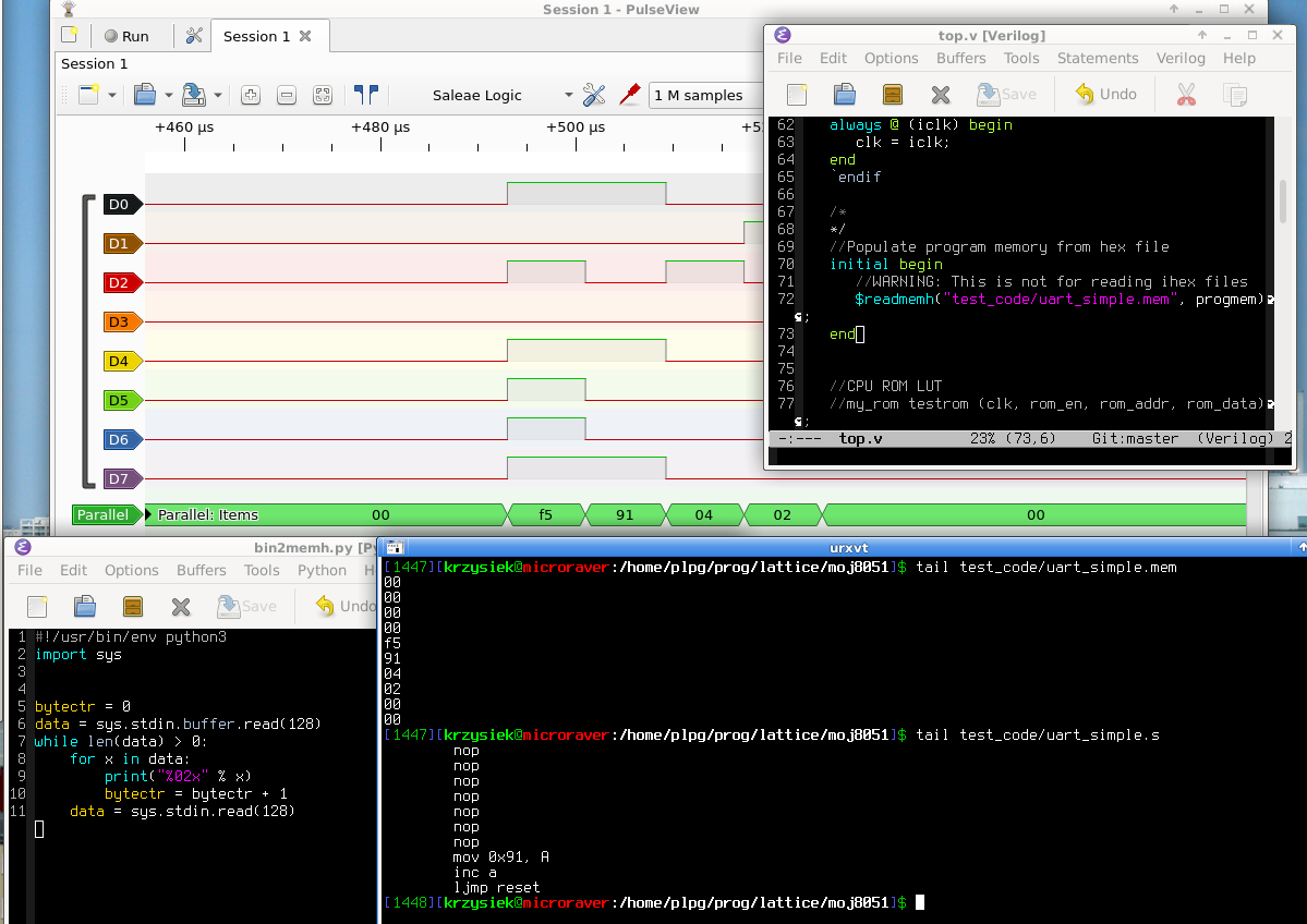
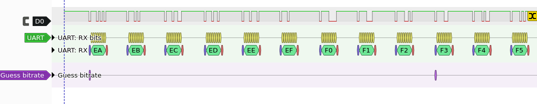
I uncommented the UART peripheral in verilog, moved one wire on the logic analyzer and it worked! Here's the UART transmitting driven by my test code that I compiled with SDCC! Uart data register is at SFR 0x91 and a write to it triggers transmission.
Unfortunately I didnt spend much time on this project recently. Writing furhter test programs revealed that, for some reason, the core does not execute conditional jumps correctly - they are always taken, regardless of the condition. I dont have time to dig down into it, which is a shame. I did learn a great deal while developing this, and I hope that some day I will finish this project.
To be continued
The code is available here.