Jun 2019
A reverse biased P-N junction generates some visible light, when a current is pushed through it. It's a very faint glow so it's barely noticeable at near complete dakrness. But thanks to modern photo technology we can capture it. Click on the image to view full size version. Below each image there is a description of it.
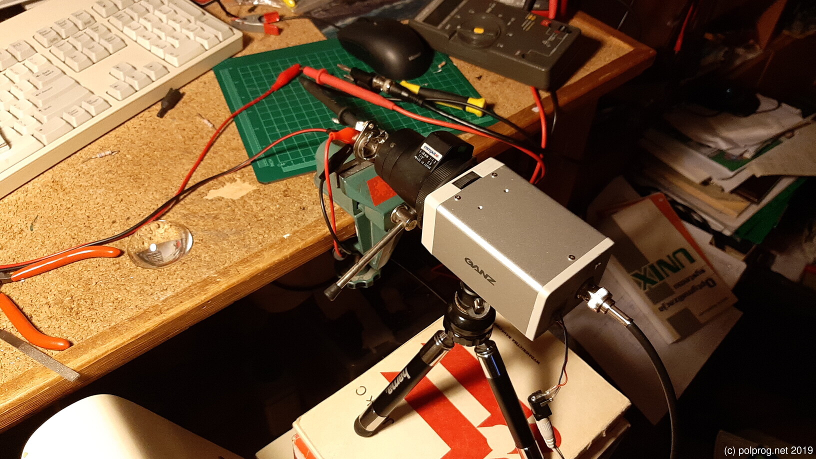
I decided to try this experiment myself and take some pictures having read this twitter thread. I've wanted to get into technical photography for quite some time now, and this turned out to be a great opportunity. I have taken some visible spectrum photos using my Canon Powershot G9. Then I set up a PAL CCTV camera that has a night vision function where it switches to near infrared spectrum and connected it to a video capture card described here. I wanted to take some macro pictures of the electroluminescence effect at the junction and some IR images as well.
This post is divided into the following sections Setup — Lower current — Higher current — Visible+IR photos — Summary
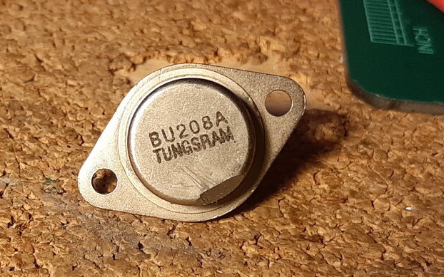
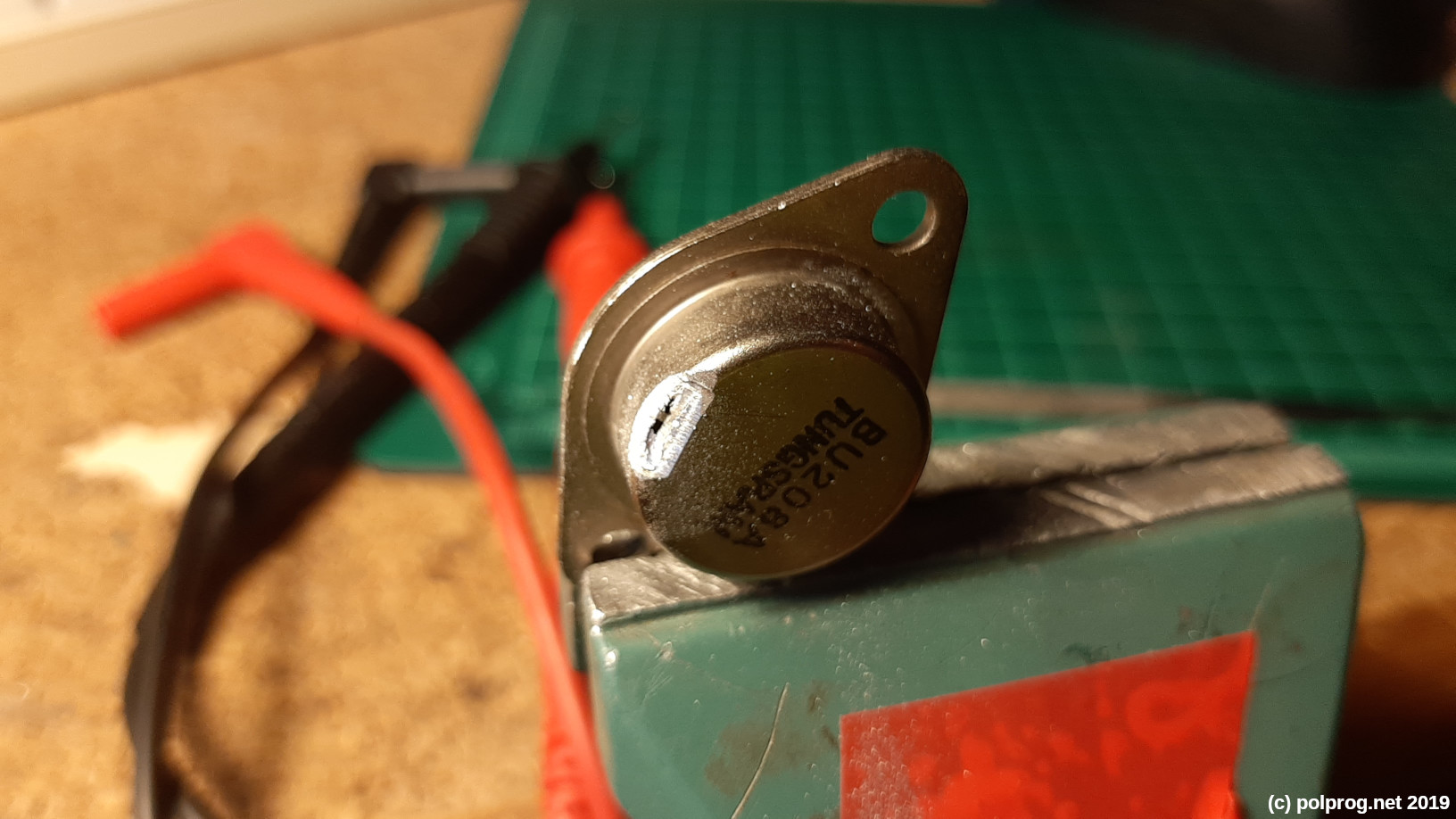
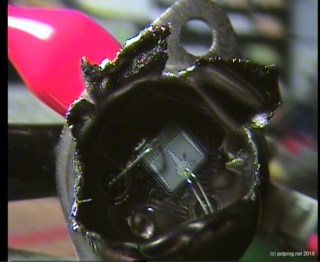
In my parts drawer I found a BU208A power NPN transistor. It had a metal TO-3 case, and as such made a perfect experimental device.
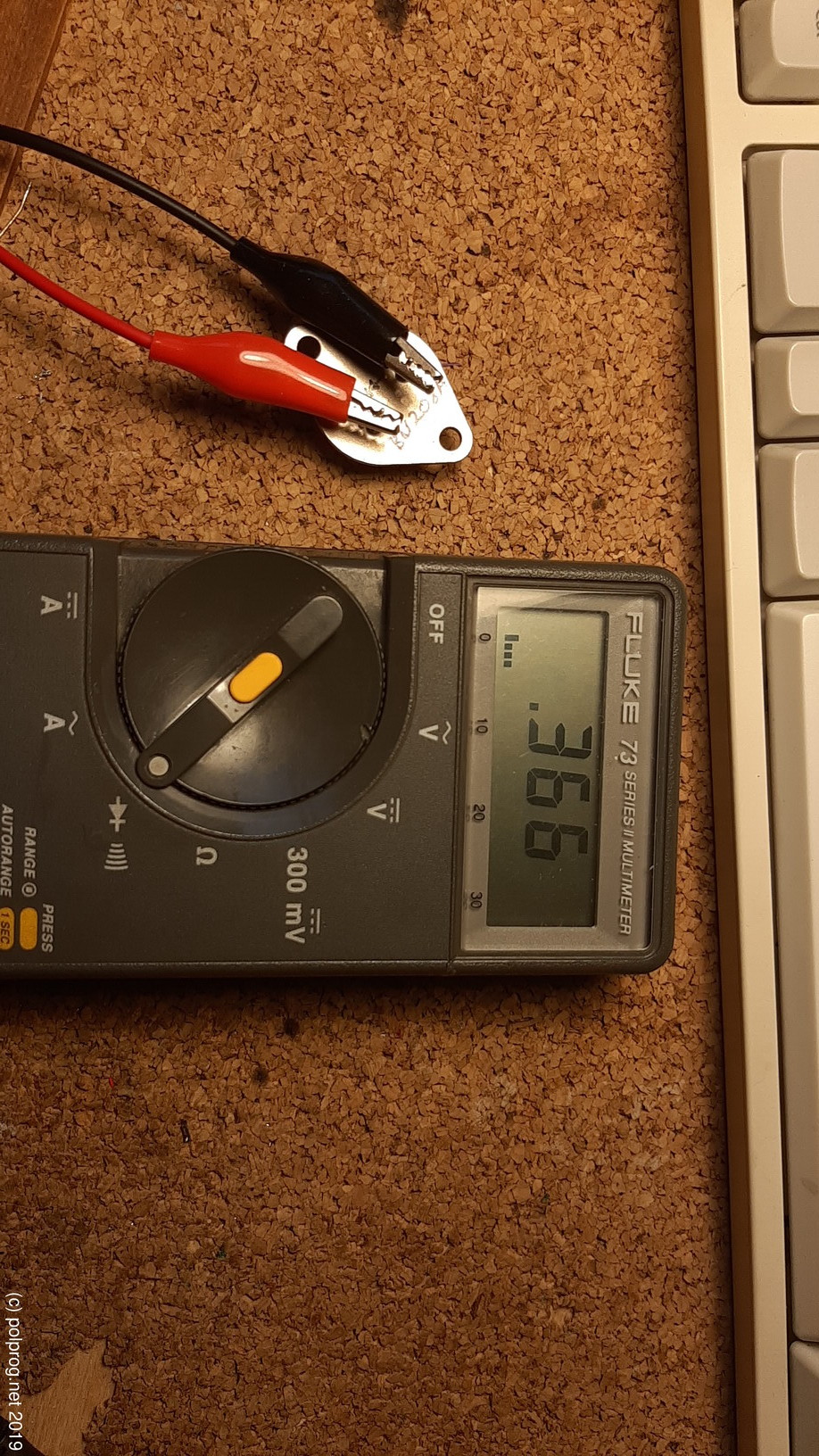
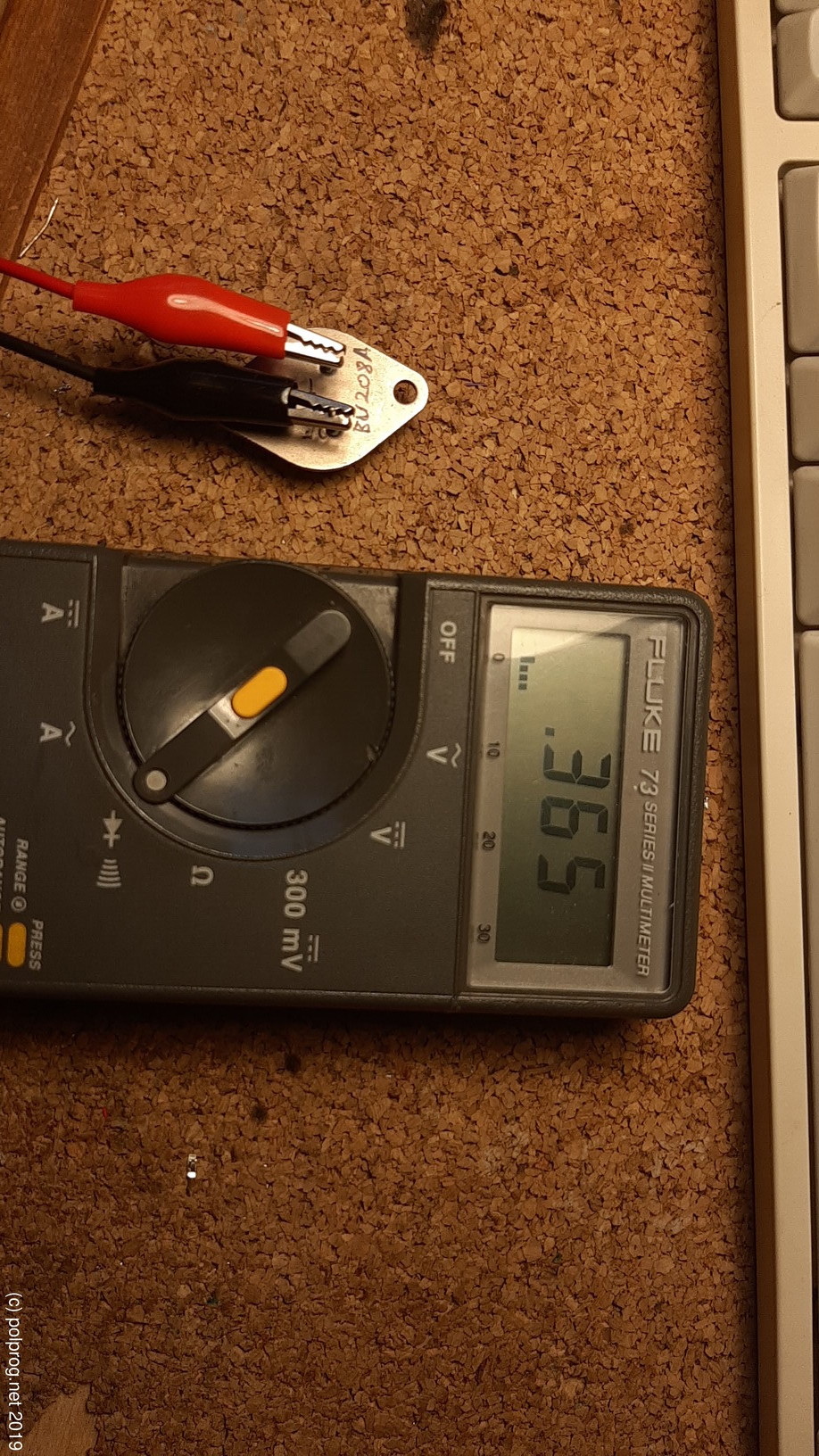
I started by measuring voltage drops across the pins. Pin 1 (in the image on the left) is the base, and pin 2 is the collector. For some reason there is a .3 volts drop in both directions. I dont know where is this transistor from, but it did not cause any issue in today's experiment
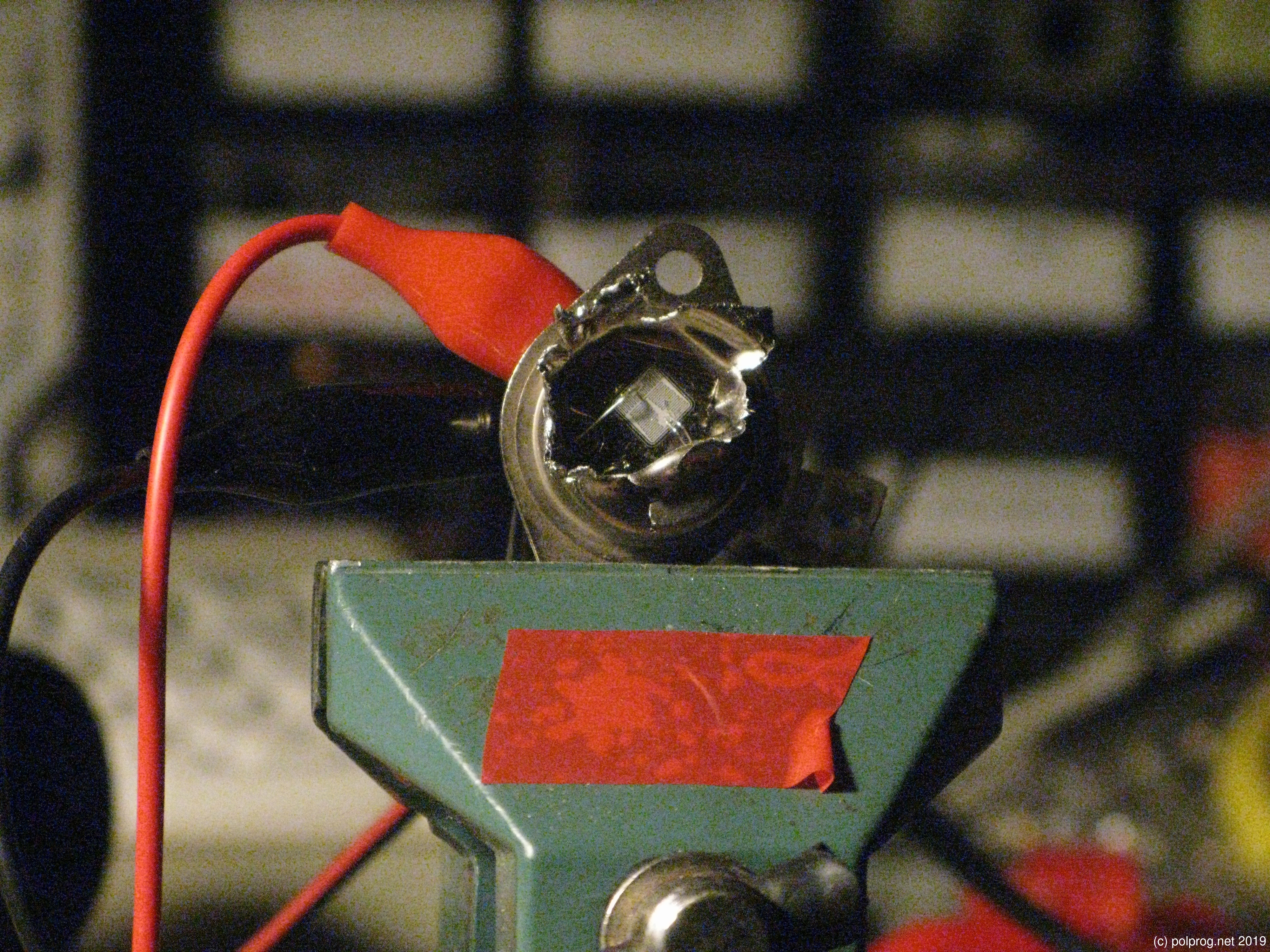
I began by grinding off the edge of the TO-3 package with a file, until the internal cavity showed up. The I inserted a flathead screwdriver to bend the top cover a little and made my way in with a pair of diagonal cutters. It's important to peel off the top part instead of cutting through it cause there is a less risk of breaking the internal bondwires.
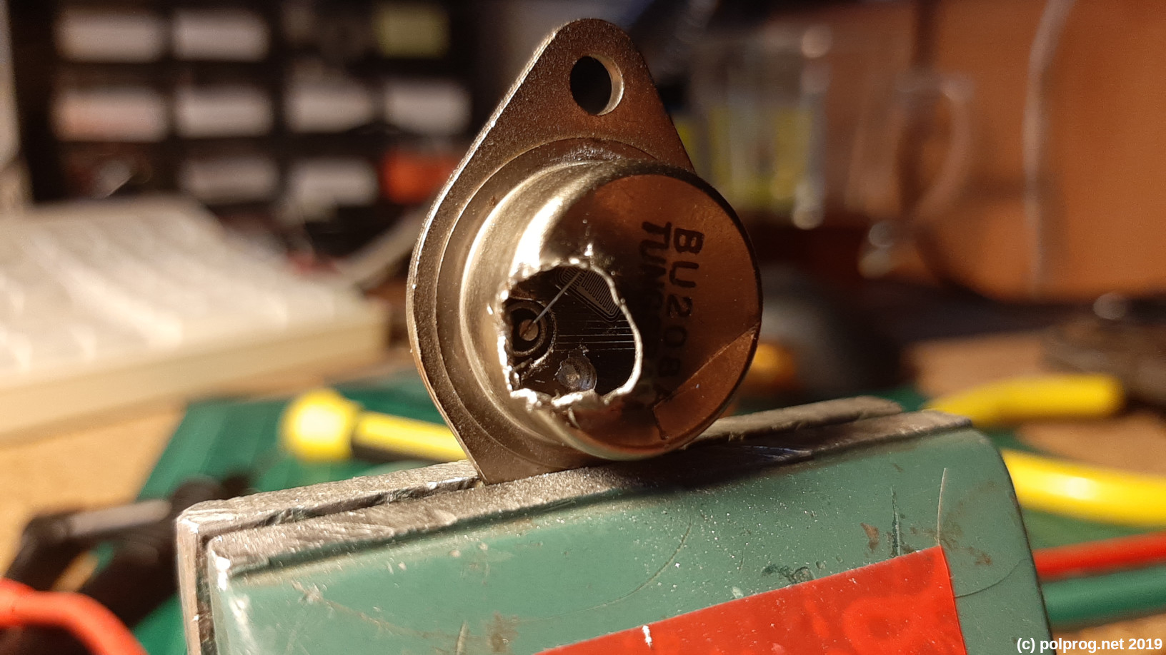
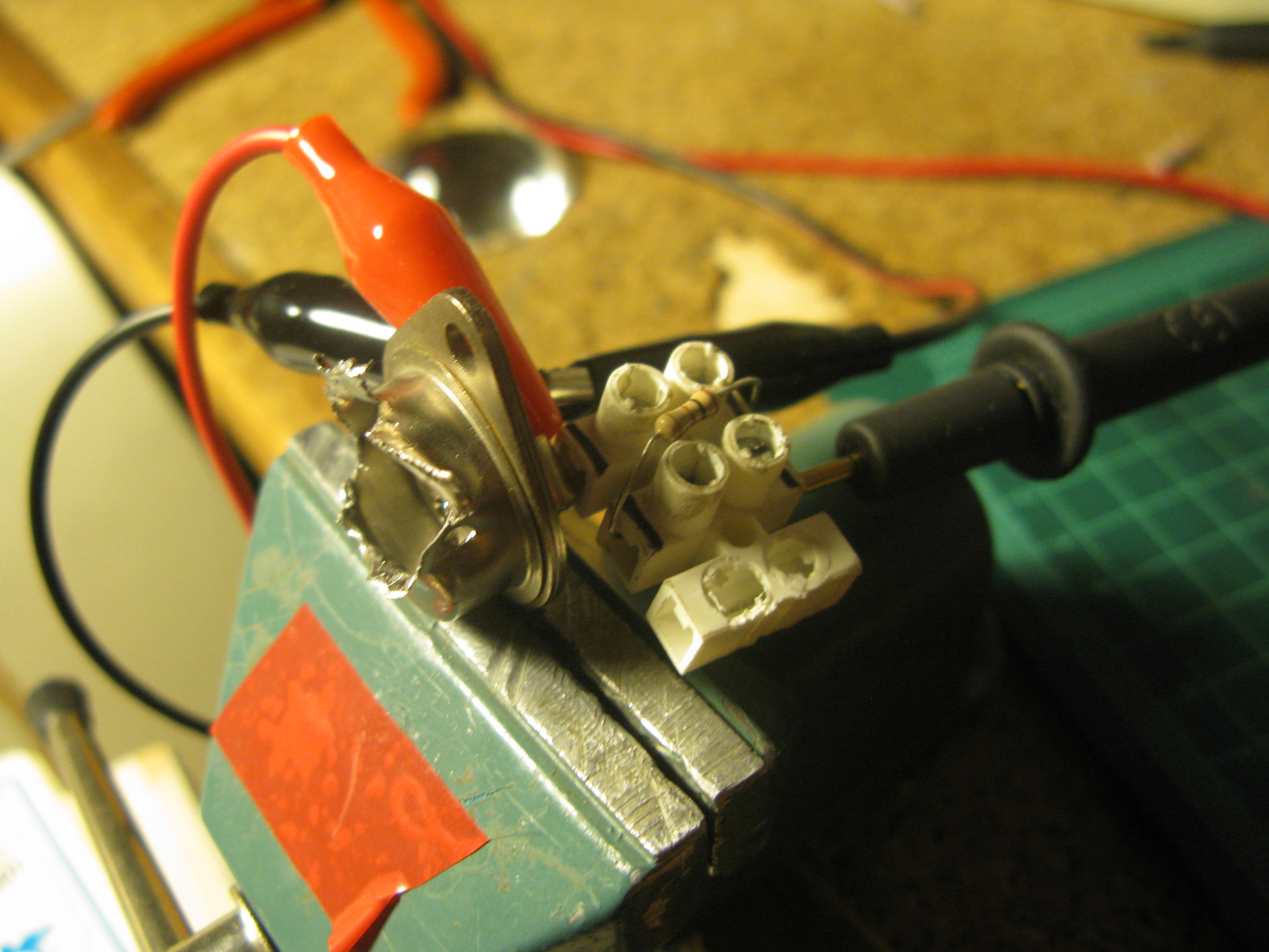
Having removed the top cover, I put the transistor in a vise...
...and built the test circuit.
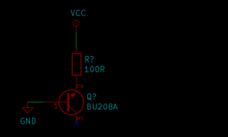
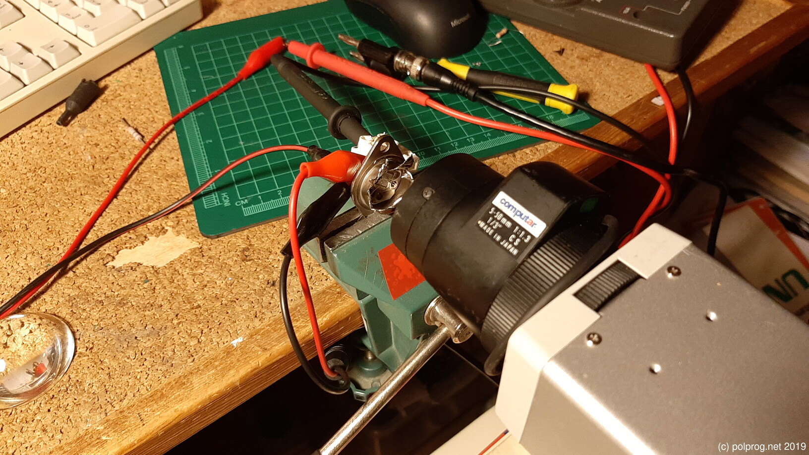
The resistor is there to limit the current, in addition to the power supply limit.
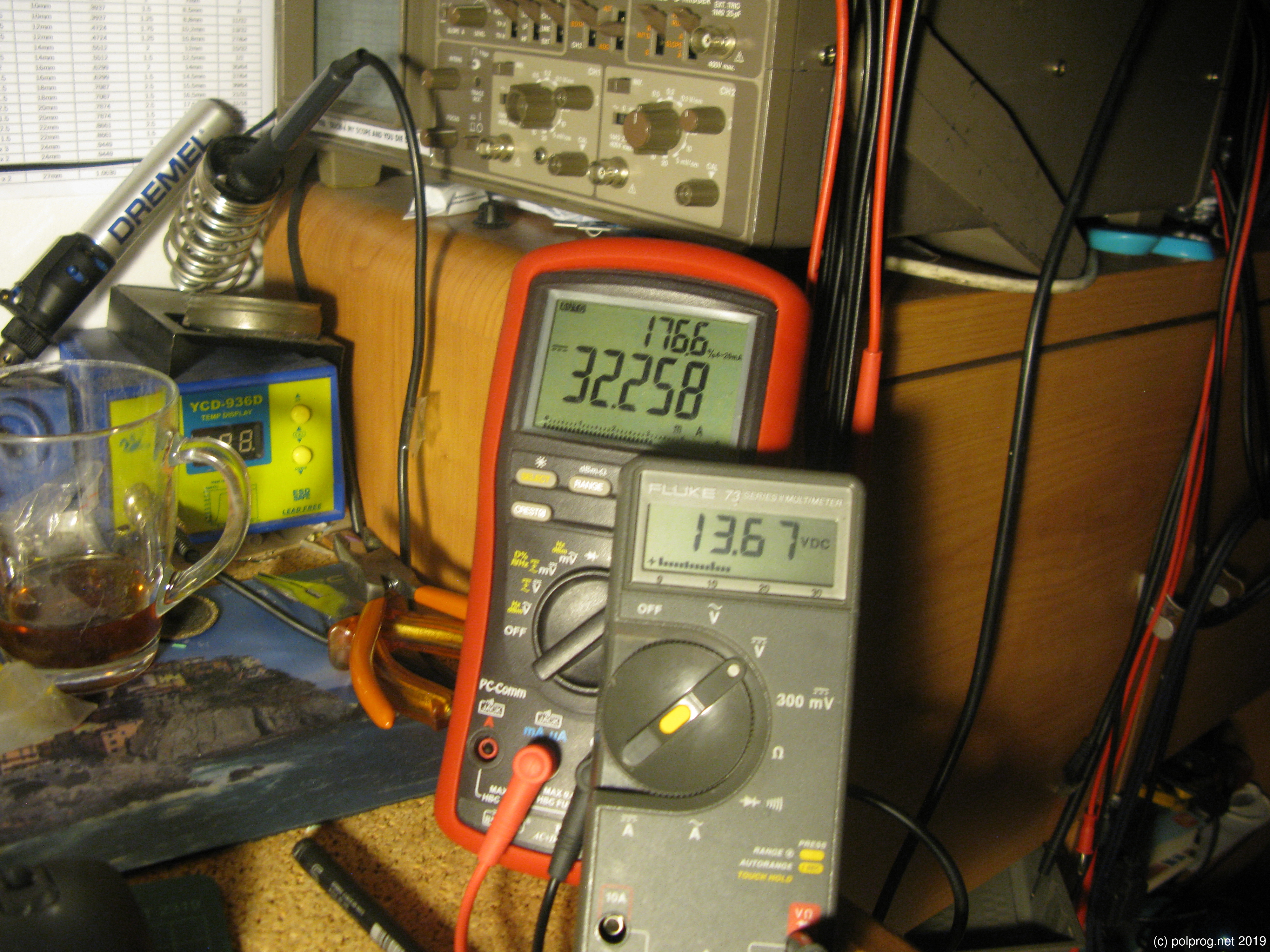
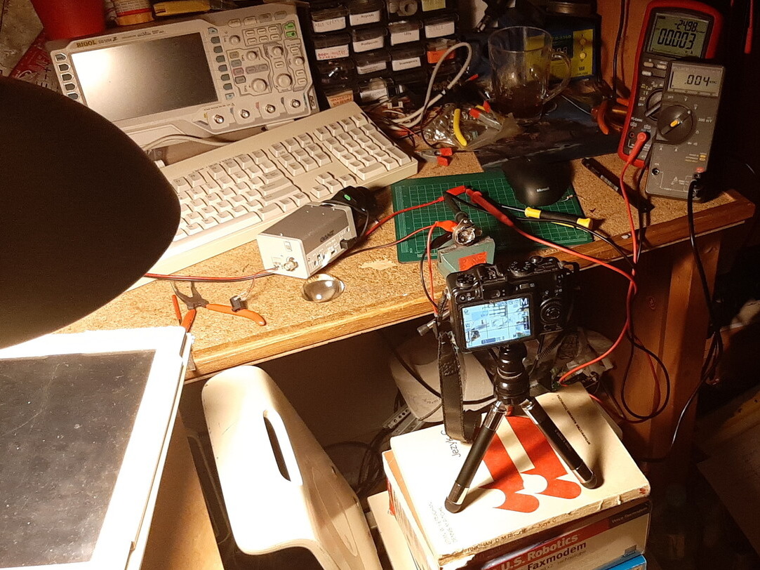
Overall, the test setup looked like this. The brymen (big red) meter measures the emitter current and the grey Fluke 73 measures the emitter-base voltage
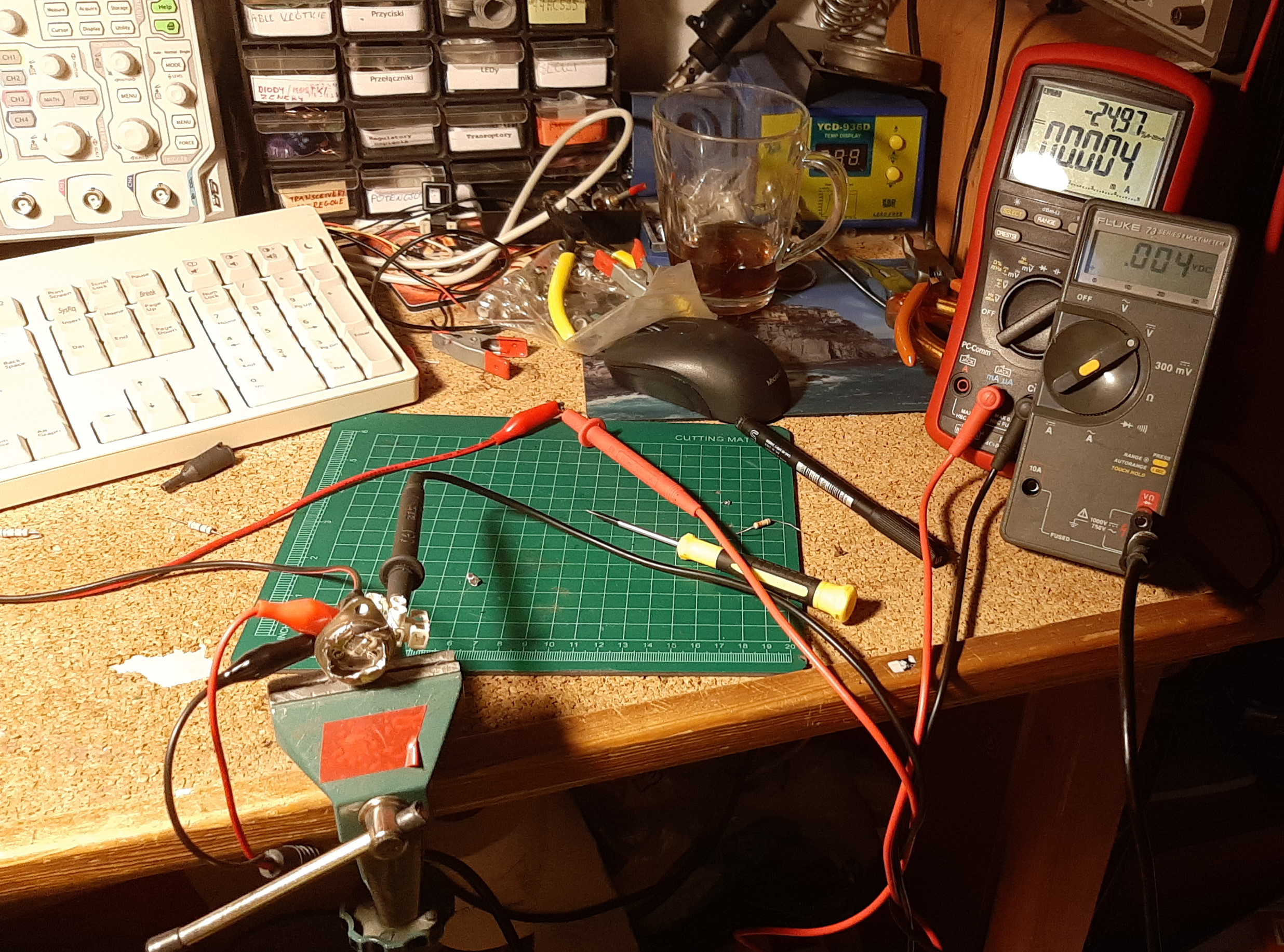
Closeup on the terminal block used to connect all the things together. The resistor is 100 ohms
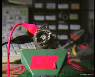
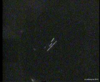
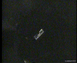
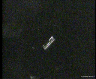
The pictures below are taken at about 30mA
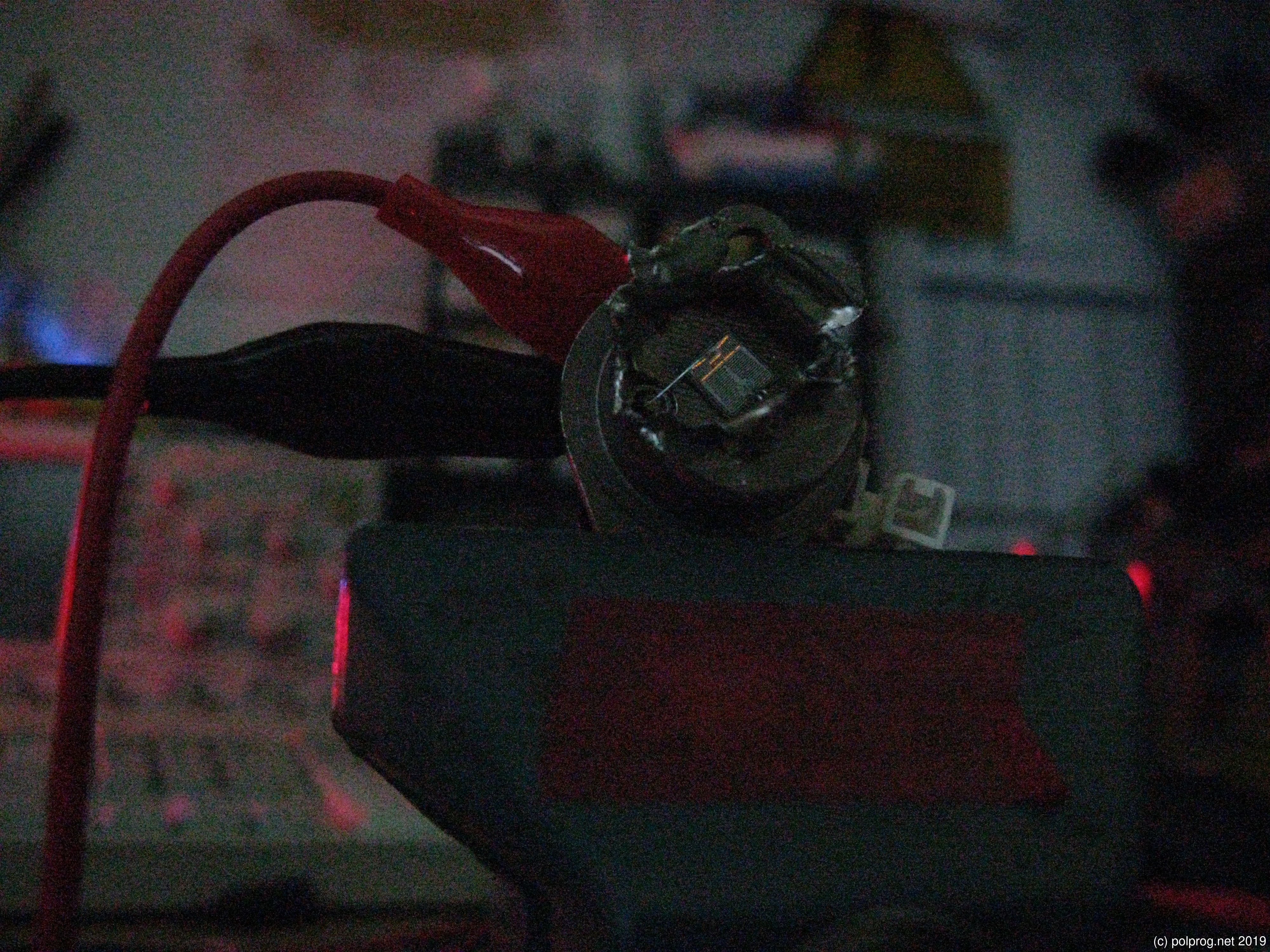
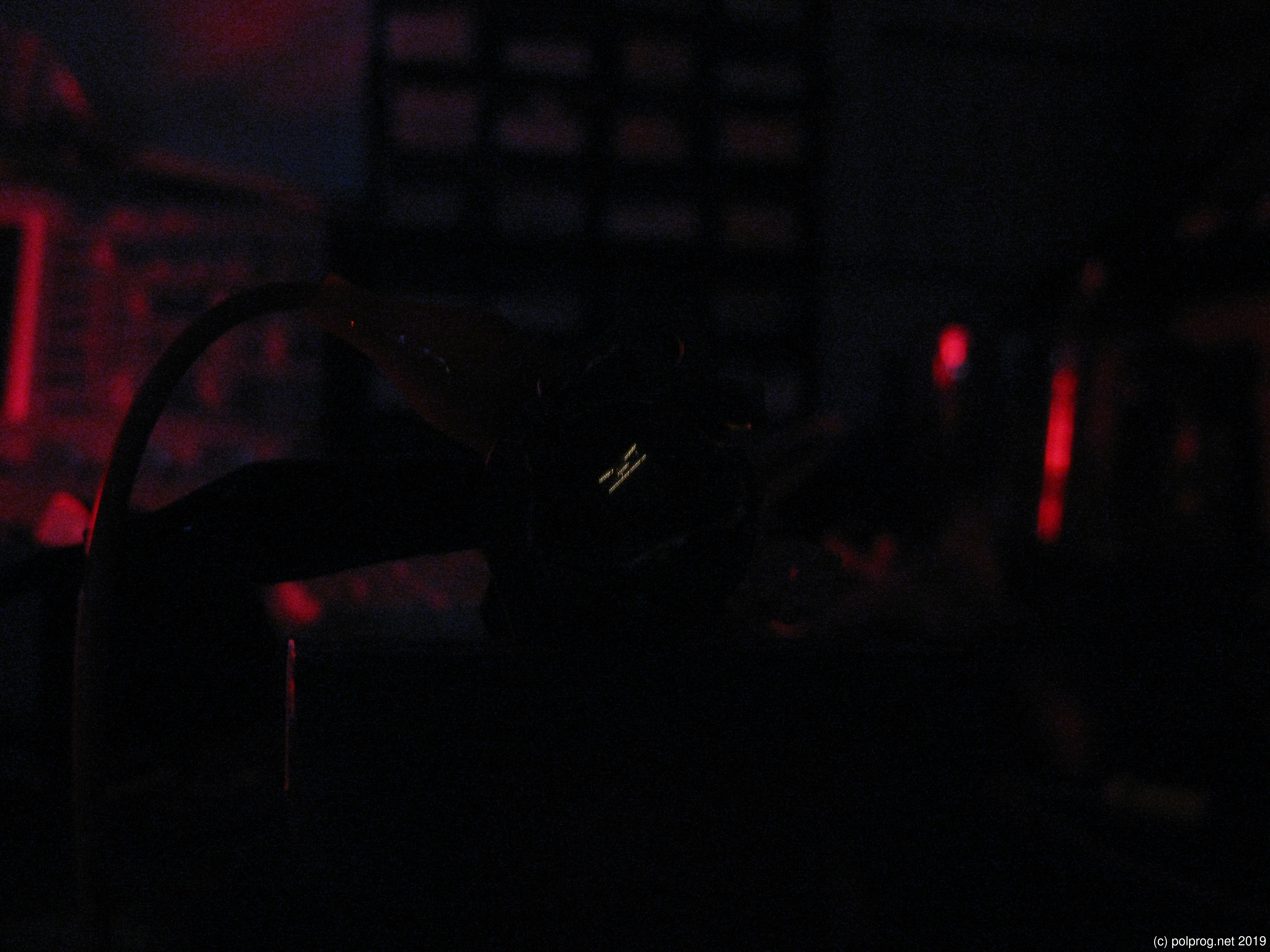
2 sec f/2.8 ISO 1600
15 sec f/3.5 ISO 400

4 sec f/3.5 ISO 1600
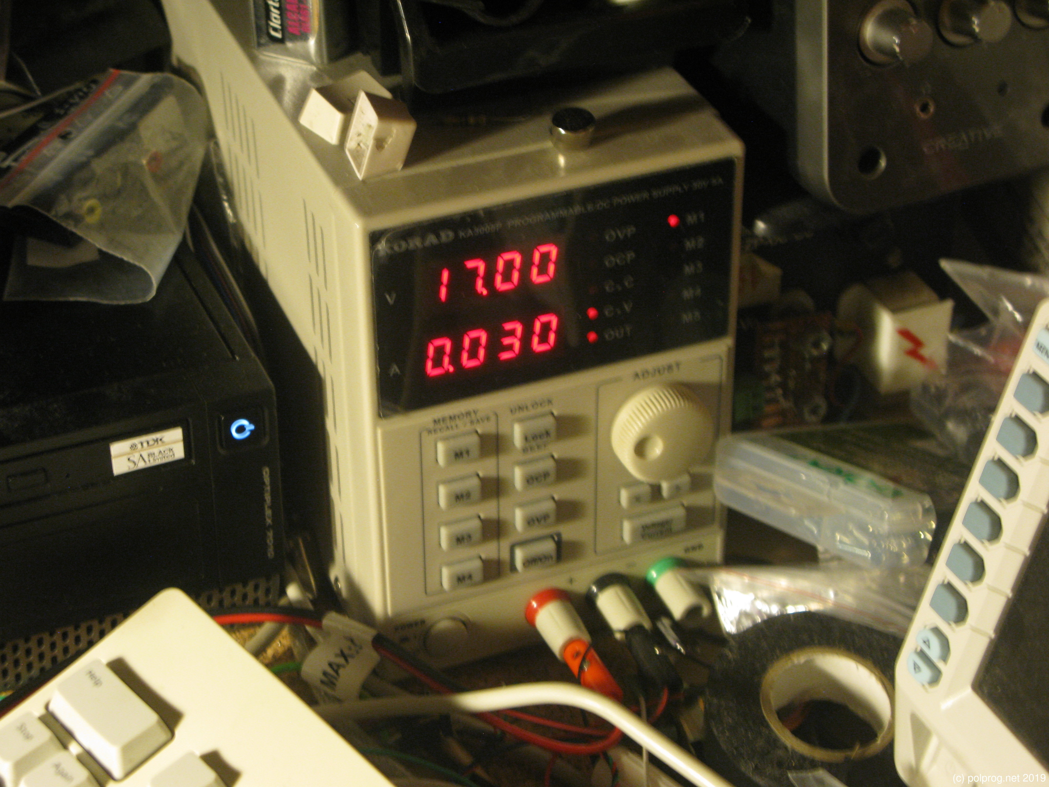
Measurements and power supply setup
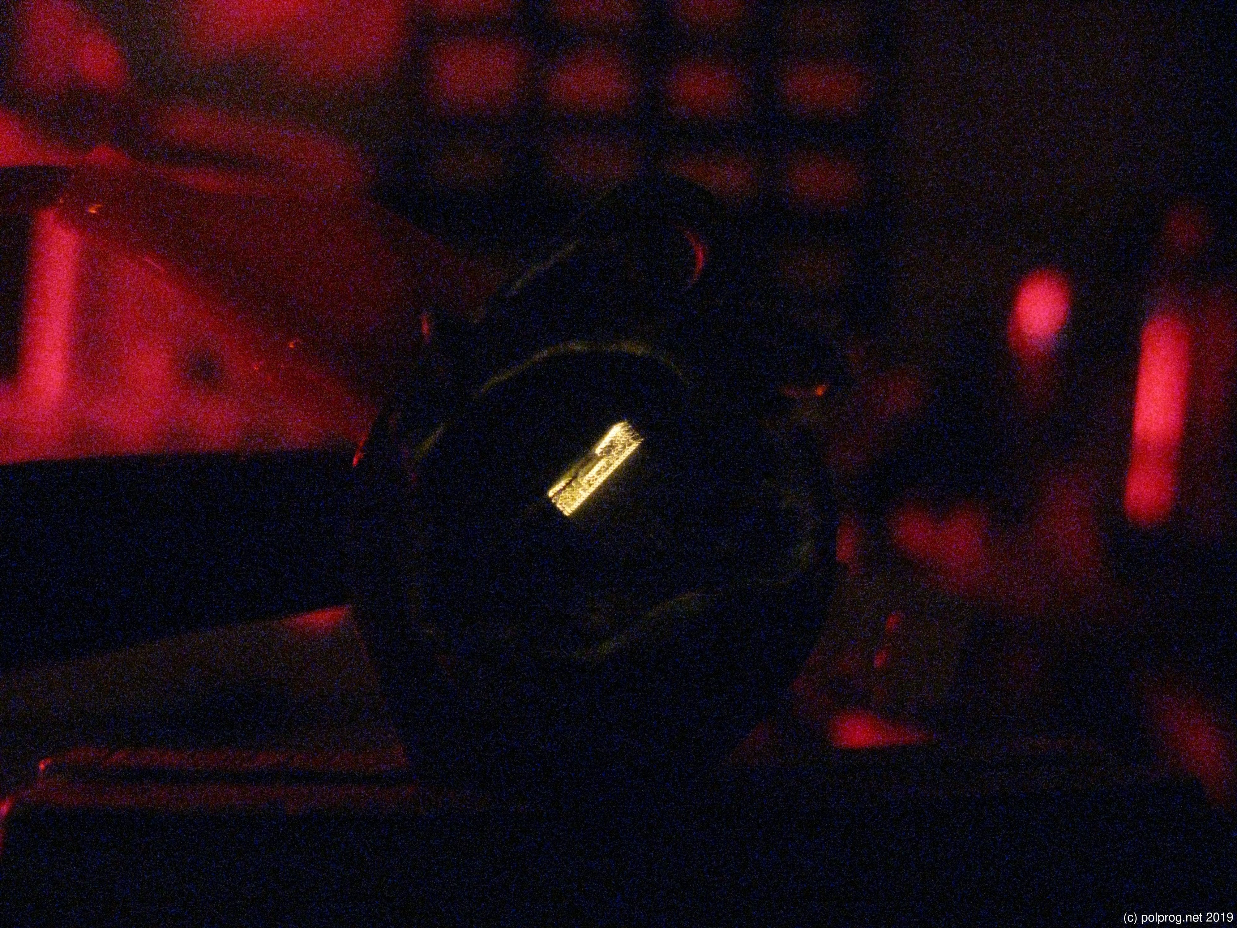
Junction at about 40mA
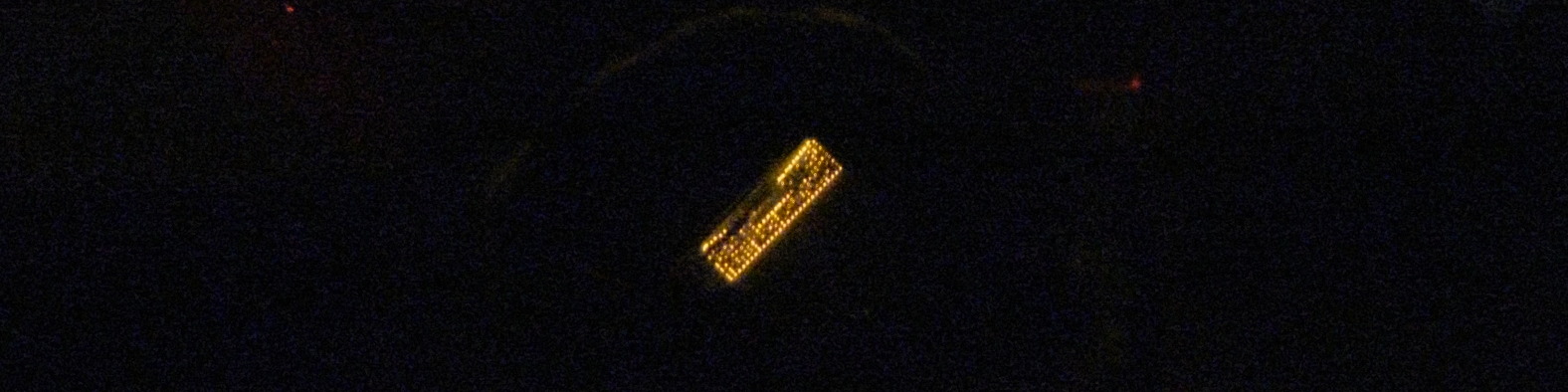
15 sec f/2.8 ISO 400. This one has got to be my favourite.
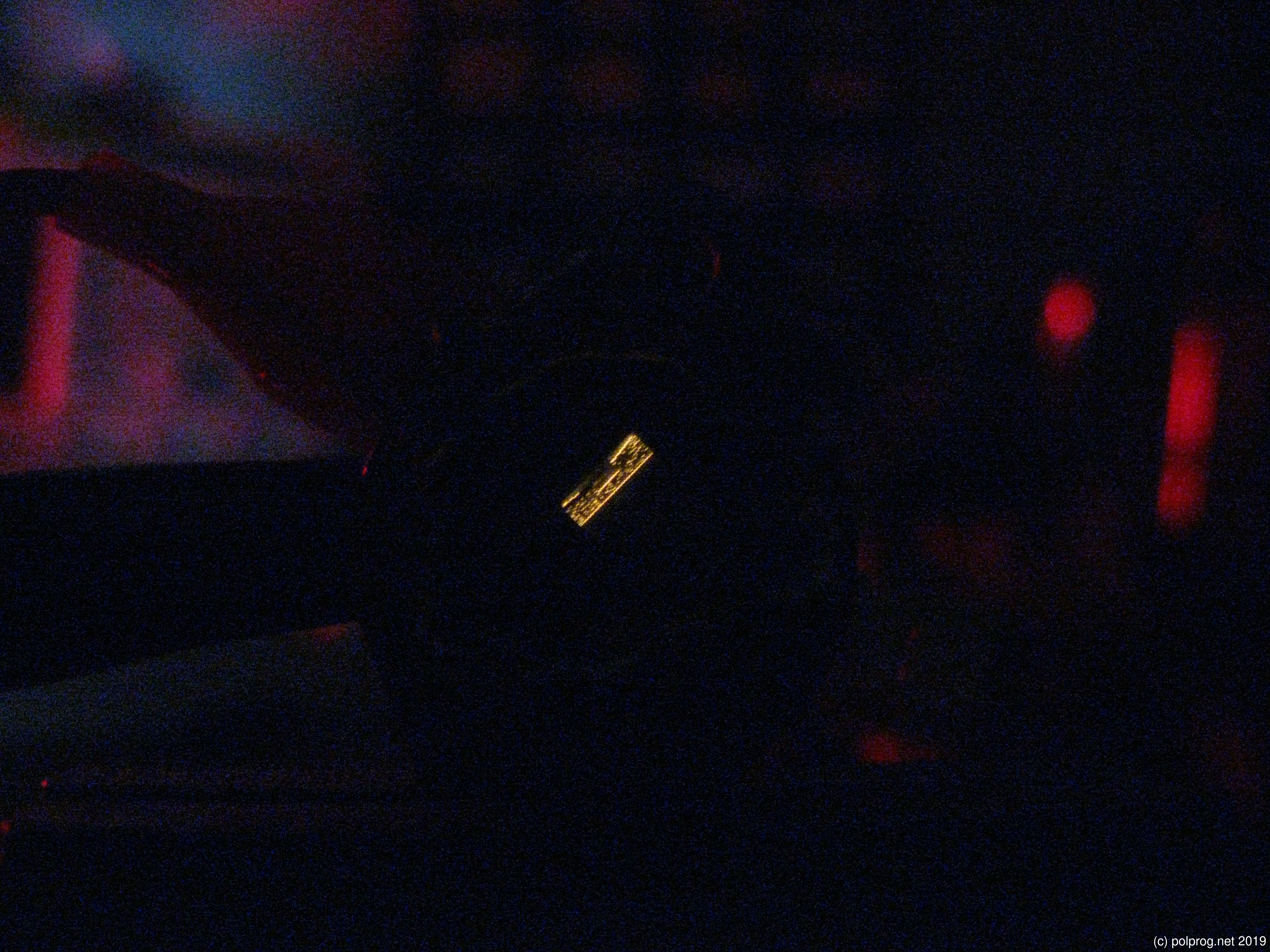
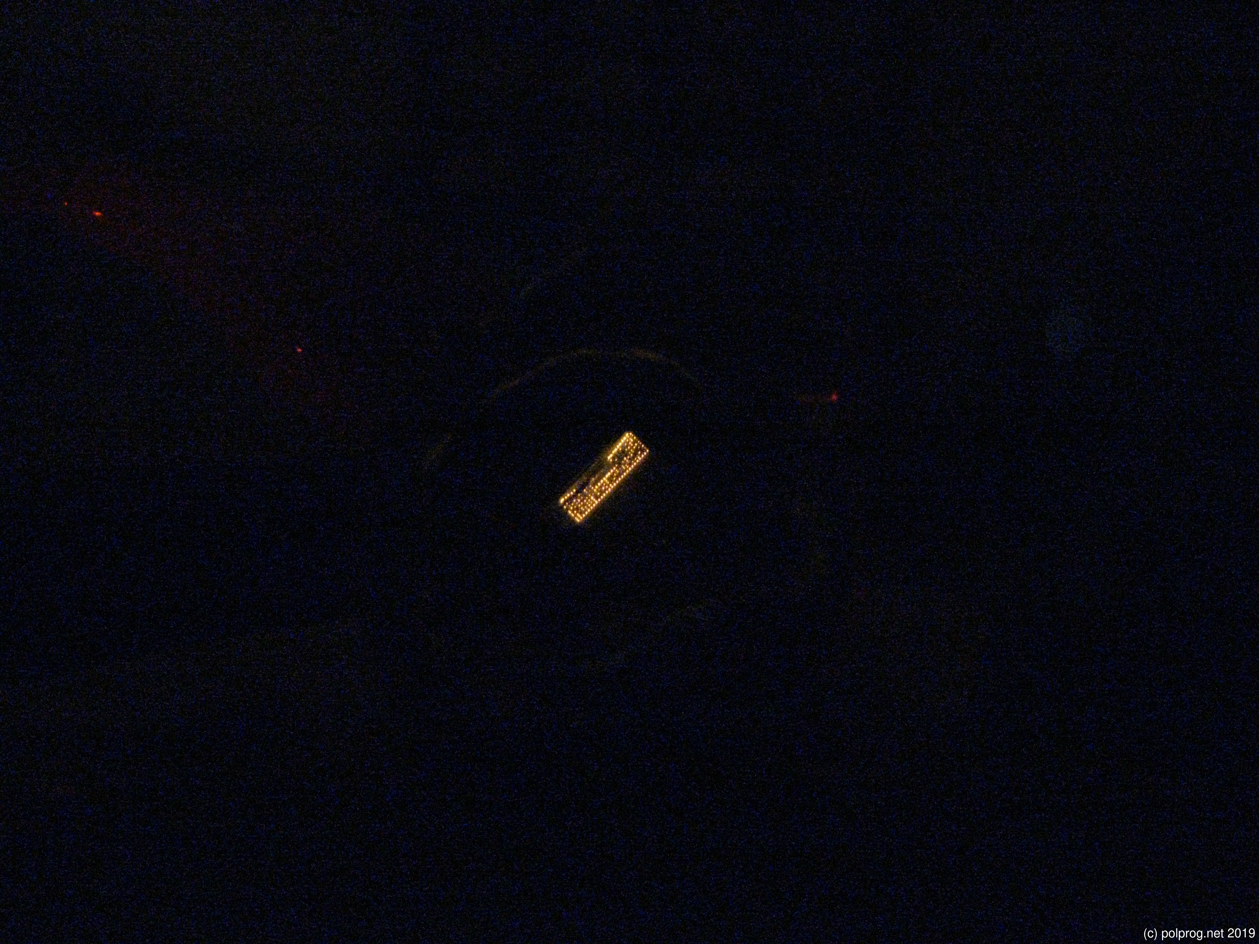
Junction at about 60mA
4 sec f/2.8 ISO 1600
15 sec f/2.8 ISO 1600
6 sec f/2.8 ISO 1600

2 sec f/2.8 ISO 1600
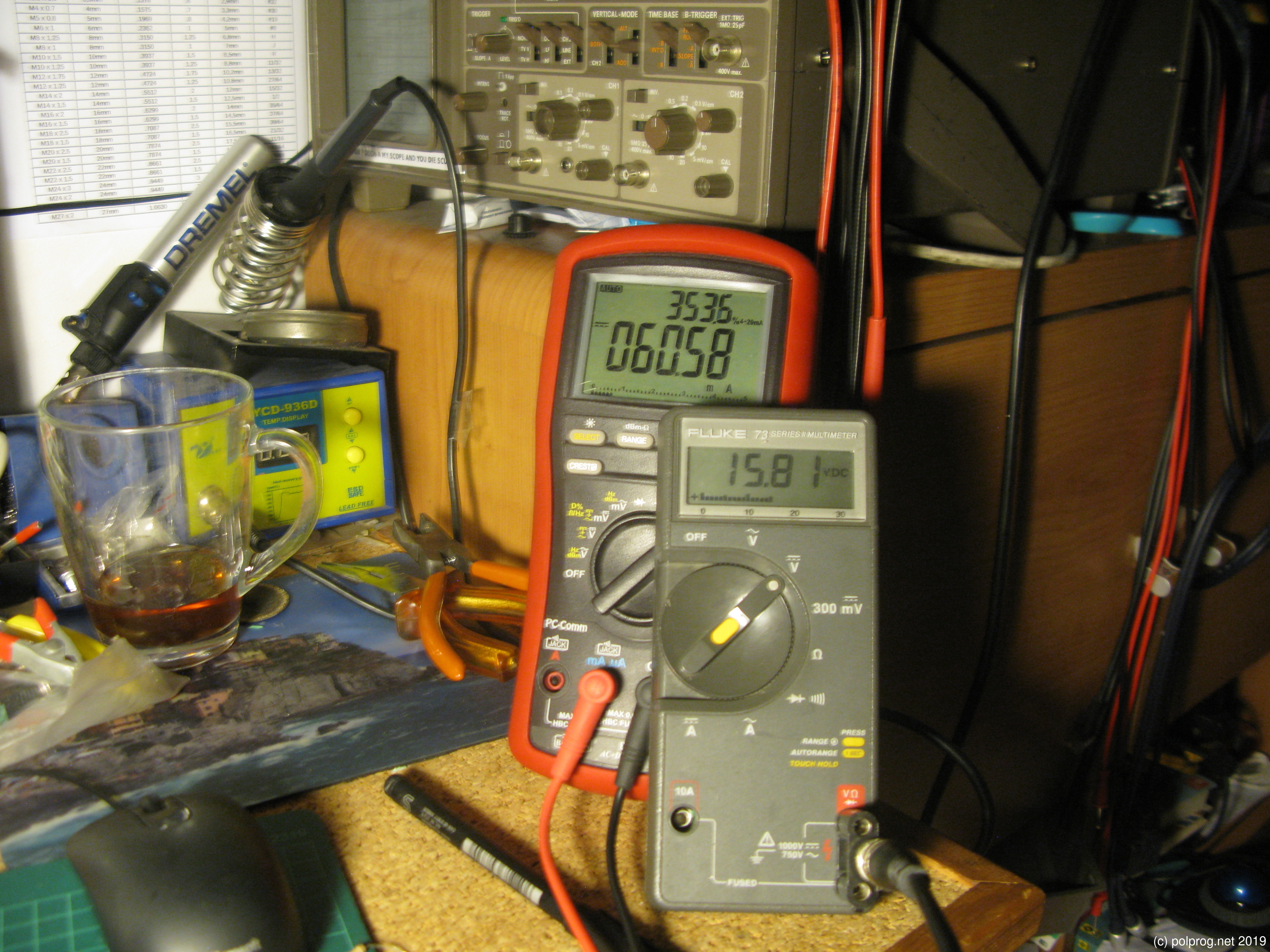

Measurements and power supply setup for 60mA
The following images were captured with a PAL CCTV camera. When the light level is too low, the camera has a night mode where it switches to visible + near-IR spectrum (on a side note, I havent found out yet how to force it to do that not based on the light level, but I digress). The camera was conencted to my quad capture card. Unfortunately the images are in PAL resolution.
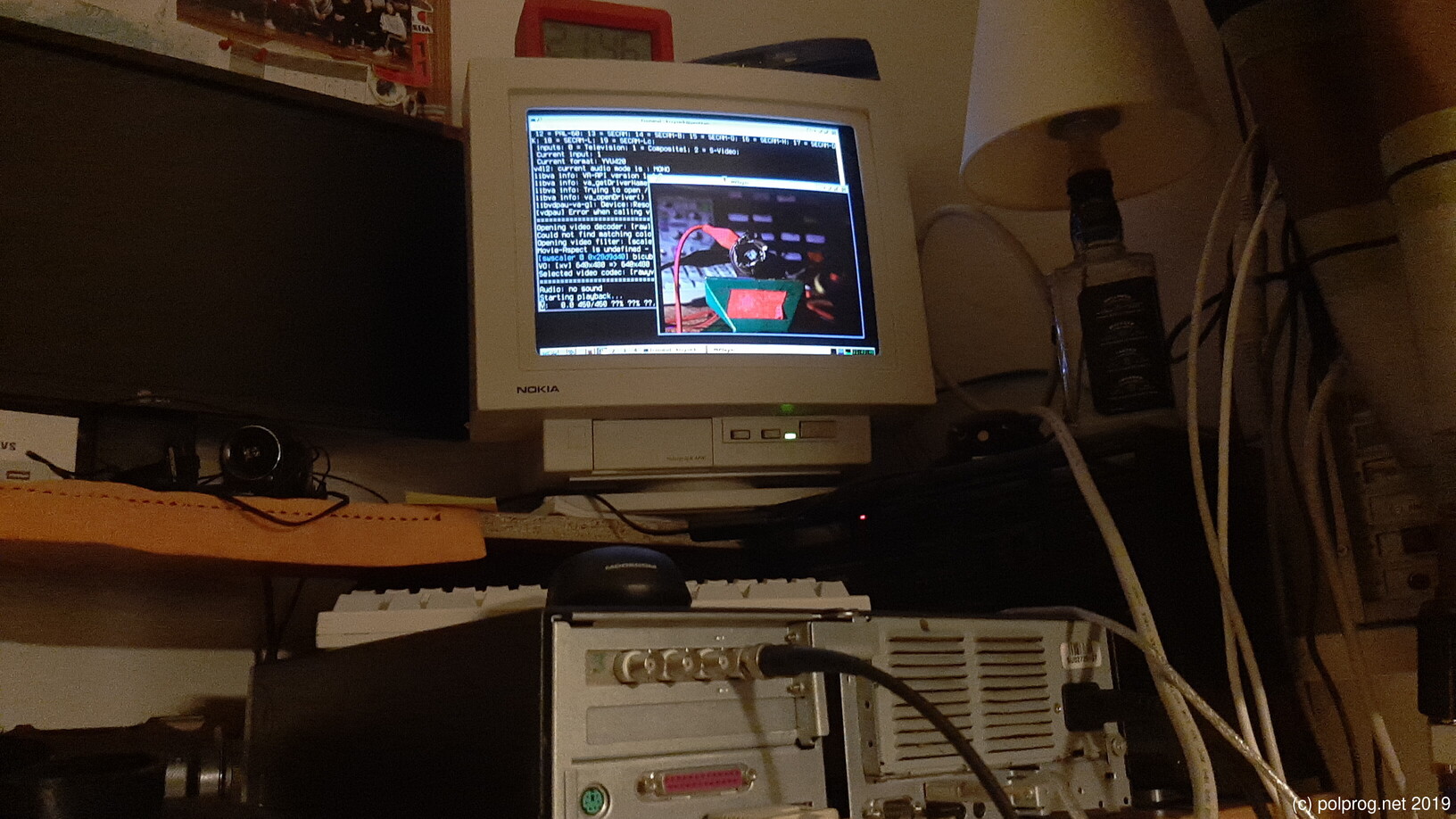
IR camera capture setup
Normal light
IR image. Junction at 30mA
IR image. Junction at 40mA
IR image. Junction at 60mA
Visible light photo setup
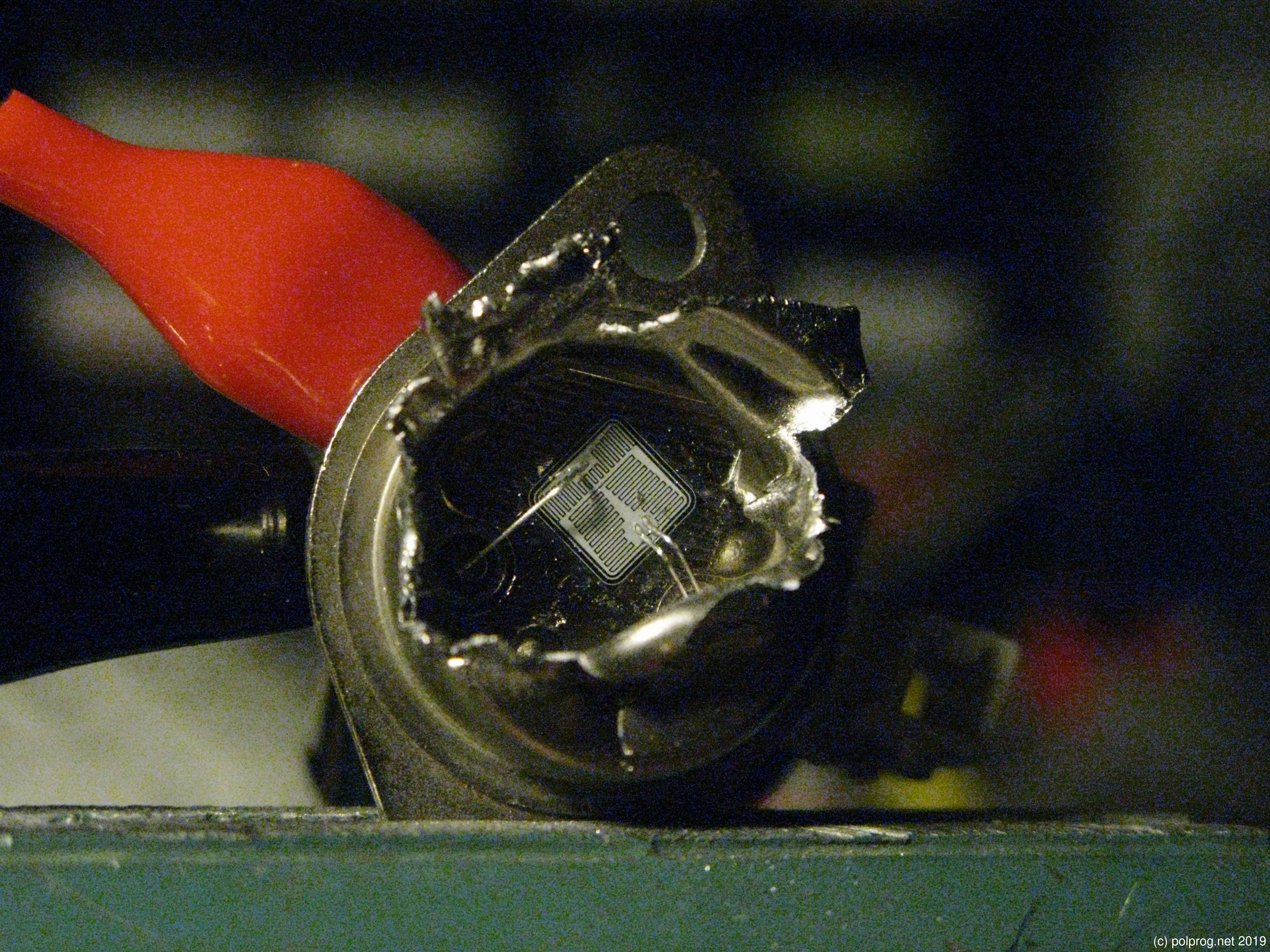
P-N junction luminescence can be captured using a relatively simple setup. The transistor used was an ordinary off-the-shelf power transistor (with a large die inside an accessible package). I have yet to determine why the P-N junction displays that specific dot pattern, however that might show where the junctions actually are on the die.
Thats it. It's easy enough to do at home and I liked this experiment a lot.
Feel free to browse my homepage, if you found this post interesting. Click on the link below to go to the homepage.