polprog 01.03.2020
I decided to give home made PCBs one more try. And it went better than I expected.
This is how I made the board, using the toner transfer method and etching in sodium persulfate.
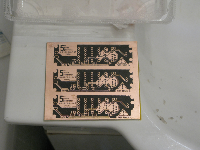
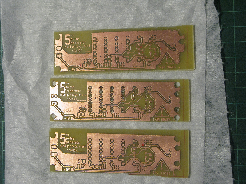
I've drawn up a small PCB for the 5ns generator project. In fact there were two revisions. The first one (left) was made in Eagle, the second in KiCad. Version 1 was never made.
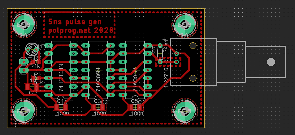
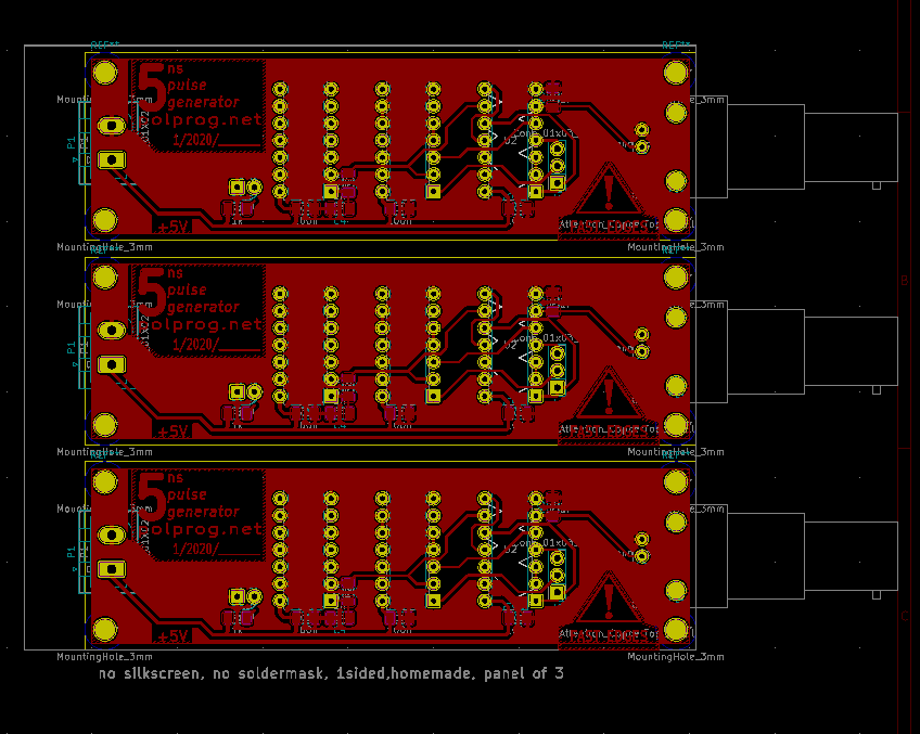
The Eagle version never got made since it was pretty much useless. I made it mostly to see if Eagle is not as cumbersome and frustratin to use as i remember it. Hint: It still sucks. The KiCad version (shown already "panelized" for the laminate size I had) came out way cleaner, in a size that allowed me to make 3 copies in one etch perfectly filling up the piece of copper clad I was going to use. I managed to sensibly fit all the components (and extra, more on that later), with minimum waste of the clad. The margin on the left is for holding the PCB while etching.
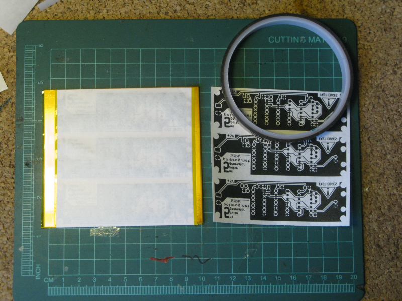
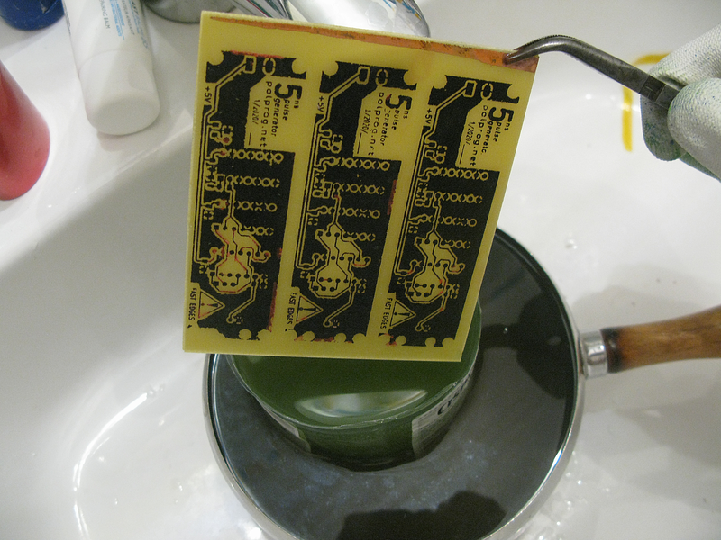
I've exported the front copper layer to PDF and printed it on special paper. It's way thinner than usual (possibly 40g/cm^2) and mid-glossy. The first print attempt ended up as a serious paper jam, so the paper needs to be manually fed into my printer. Then I cut out the printout, attached it to the copper clad with kapton tape (left image below) and transferred the toner with a clothes iron
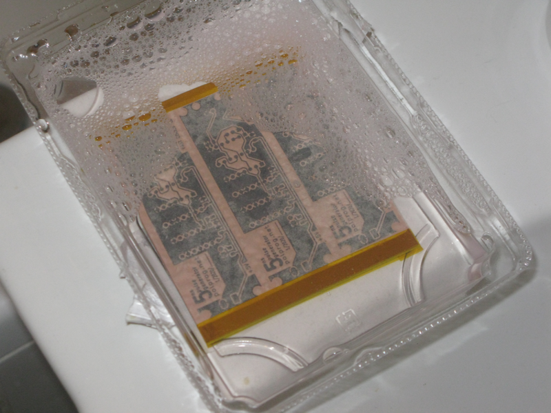
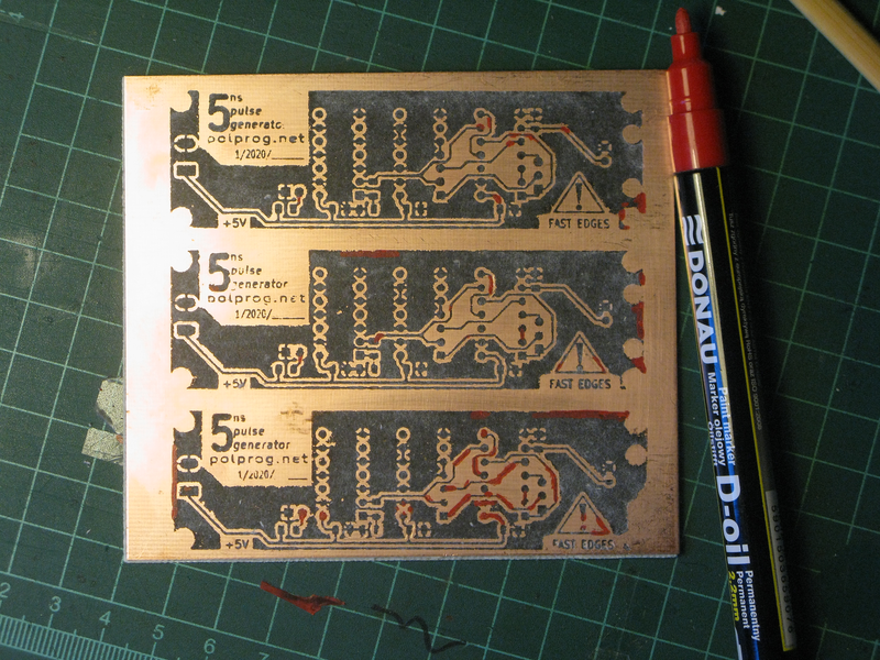
I let the PCB cool for a second and dropped it into soapy water. After 15 minutes the paper was soaked in its entirety. Then I started gently removing the paper with a soft sponge. After there was only toner left, I fixed up all the places where it did not transfer properly with a paint marker (below)
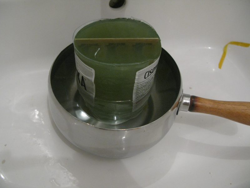
After the PCB was ready, I've mixed what I had left of the etchant in warm water. At first the etchant cooled down too quickly, and the process didn't even start. Then I've put the etching container in a pot and poured close-to-boiling water around it, creating a makeshift heated bath. The process then went okay, I've nearly overetched the board.
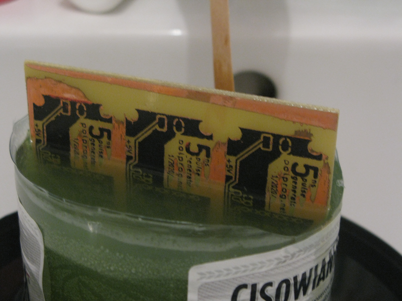
After about 10 minutes the board was ready (bottom left) to stop the process and remove the toner. Isopropanol is good for the task, as well as acetone. I've used the former.
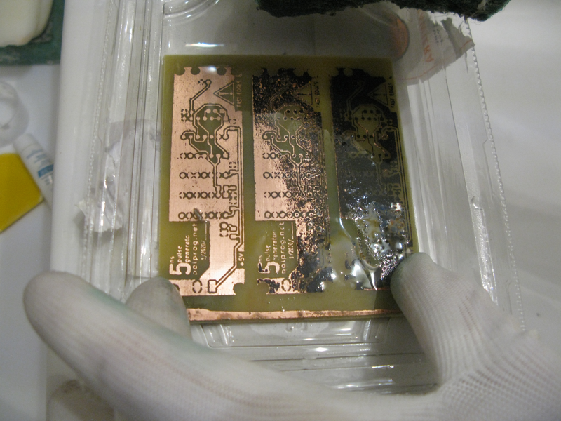
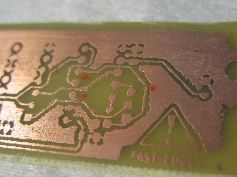
Ive dropped the board into the tray that was used for the soapy water before, now filled with a little isopropanol, and used the rough side of a sponge to remove the toner. Next up, quality control. I've marked all the places where the traces were overetched with the paint marker so that I know what to fix up when soldering.
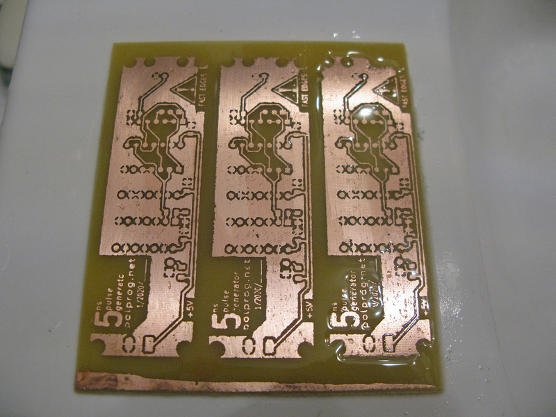
Then I drilled the holes. Four corner mounting holes are 3mm in diameter. BNC connector support holes were made with a 2mm drill, and all the rest (DIPs, pin headers, etc.) with a 1mm drill.
Making a PCB that's meant to be home etched is quite different from making one that is meant to go to a fab. Here are some things to keep in mind when doing so.
First of all, this PCB was single sided. (It's possible to make double sided PCBs at home, but it's more hassle than it's worth in my opinion.) That means no vias, and more demanding trace routing. I had to swap the arrangement of the 4 inverters used in this project to make it easy to route.
I laid out the ICs in a way that it would be easy to route Vcc and GND to. That means all of them were aligned in the same direction, with signals flowing left to right. Each of the ICs has a 100n decoupling cap next to VCC. The bus going along the line is not the best possible power delivery topology, but it's the most optimal for this PCB size and shape. Since GND was to be filled, the VCC trace were a little wider.
Grounding was first done manually in a star topology, with grounds going horizontally connecting several ground pins (mostly unused inputs of the CMOS ICs). Then I added a copper pour for the ground net. This way, by first doing ground with traces, you make sure all the ground were connected. A copper fill may make two separate planes which is easy to miss (but shows up on DRC).
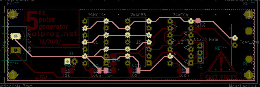
Initially, all three main ground traces met close to the power input. But then when I was adding the text, the ground fill was in place, so I deleted some of these traces. This caused a small thin stripe of ground left between the HCT16 and the text, but that did not cause any issues on the final board.
Then I routed sub-units like the output stage, or the RC circuit around the HCT14, next up were the traces interconnecting the ICs. Finally, some fine tuning. To fit the text I extended the board a little to the left, and moved the power input there. I've also moved the BNC a little to make space for the mounting holes and the warning sign.
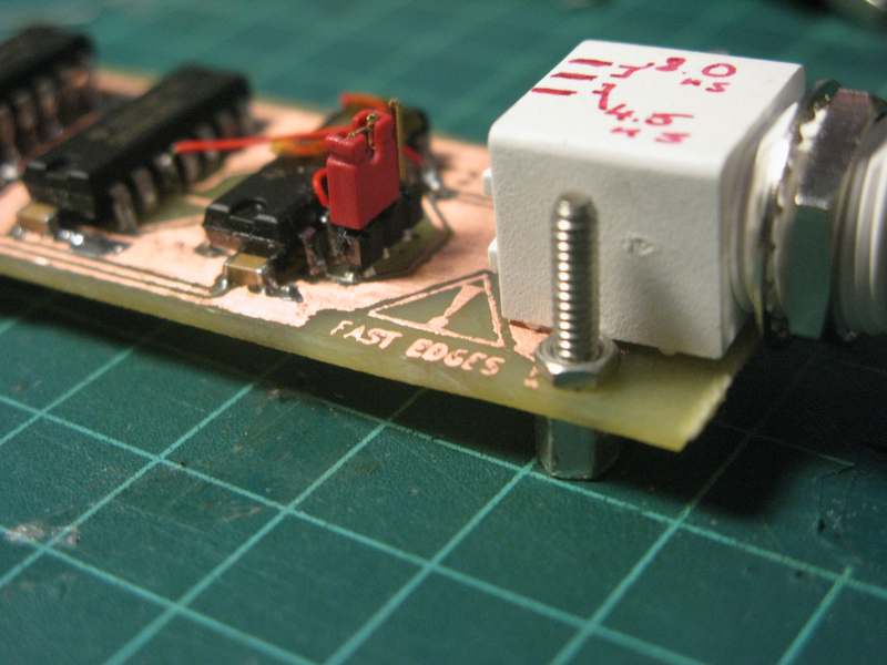
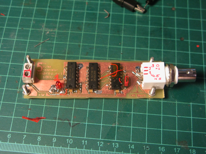
Earlier, when drawing the schematic, I've noticed I have three spare inverters in the AC04. Using them I've added a 3 pin jumper that allows to select between 2 or 4 inverters in the delay chain (see theory of operation). This allows to select between 8 and 4 ns pulse width.
I also made a mistake while drawin the schematic based off the breadboard, and missed one inverter in the output stage.. The XOR has different polarity than the schematic so after I built the PCB, the ouput pulses were of the wrong polarity. A jumper wire and a cut trace "fixed" that, but now the XOR is driving the output, and I'm getting different peak voltage. This will have to be fixed in the next PCB.